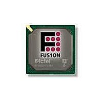
AFS600-FGG256 Actel, AFS600-FGG256 Datasheet - Page 242

AFS600-FGG256
Manufacturer Part Number
AFS600-FGG256
Description
FPGA - Field Programmable Gate Array 600K System Gates
Manufacturer
Actel
Datasheet
1.AFS600-PQG208.pdf
(330 pages)
Specifications of AFS600-FGG256
Processor Series
AFS600
Core
IP Core
Maximum Operating Frequency
1098.9 MHz
Number Of Programmable I/os
119
Data Ram Size
110592
Supply Voltage (max)
1.575 V
Maximum Operating Temperature
+ 70 C
Minimum Operating Temperature
0 C
Development Tools By Supplier
AFS-Eval-Kit, AFS-BRD600, FlashPro 3, FlashPro Lite, Silicon-Explorer II, Silicon-Sculptor 3, SI-EX-TCA
Mounting Style
SMD/SMT
Supply Voltage (min)
1.425 V
Number Of Gates
600 K
Package / Case
FPBGA-256
Lead Free Status / RoHS Status
Lead free / RoHS Compliant
Available stocks
Company
Part Number
Manufacturer
Quantity
Price
Company:
Part Number:
AFS600-FGG256
Manufacturer:
Actel
Quantity:
135
Part Number:
AFS600-FGG256
Manufacturer:
ACTEL/爱特
Quantity:
20 000
Company:
Part Number:
AFS600-FGG256I
Manufacturer:
Microsemi SoC
Quantity:
10 000
Company:
Part Number:
AFS600-FGG256K
Manufacturer:
Microsemi SoC
Quantity:
10 000
- Current page: 242 of 330
- Download datasheet (13Mb)
Device Architecture
2- 22 6
pump, and eNVM operation. VCCOSC is off only when VCCA is off. VCCOSC must be powered
whenever the Fusion device needs to function.
VCC
Supply voltage to the FPGA core, nominally 1.5 V. VCC is also required for powering the JTAG state
machine, in addition to VJTAG. Even when a Fusion device is in bypass mode in a JTAG chain of
interconnected devices, both VCC and VJTAG must remain powered to allow JTAG signals to pass
through the Fusion device.
VCCIBx
Supply voltage to the bank's I/O output buffers and I/O logic. Bx is the I/O bank number. There are either
four (AFS090 and AFS250) or five (AFS600 and AFS1500) I/O banks on the Fusion devices plus a
dedicated V
Each bank can have a separate VCCI connection. All I/Os in a bank will run off the same VCCIBx supply.
VCCI can be 1.5 V, 1.8 V, 2.5 V, or 3.3 V, nominal voltage. Unused I/O banks should have their
corresponding VCCI pins tied to GND.
VCCPLA/B
Supply voltage to analog PLL, nominally 1.5 V, where A and B refer to the PLL. AFS090 and AFS250
each have a single PLL. The AFS600 and AFS1500 devices each have two PLLs. Actel recommends
tying VCCPLX to VCC and using proper filtering circuits to decouple VCC noise from PLL.
If unused, VCCPLA/B should be tied to GND.
VCOMPLA/B
VCOMPLA is the ground of the west PLL (CCC location F) and VCOMPLB is the ground of the east PLL
(CCC location C).
VJTAG
Fusion devices have a separate bank for the dedicated JTAG pins. The JTAG pins can be run at any
voltage from 1.5 V to 3.3 V (nominal). Isolating the JTAG power supply in a separate I/O bank gives
greater flexibility in supply selection and simplifies power supply and PCB design. If the JTAG interface is
neither used nor planned to be used, the VJTAG pin together with the TRST pin could be tied to GND. It
should be noted that VCC is required to be powered for JTAG operation; VJTAG alone is insufficient. If a
Fusion device is in a JTAG chain of interconnected boards and it is desired to power down the board
containing the Fusion device, this may be done provided both VJTAG and VCC to the Fusion part remain
powered; otherwise, JTAG signals will not be able to transition the Fusion device, even in bypass mode.
VPUMP
Fusion devices support single-voltage ISP programming of the configuration flash and FlashROM. For
programming, VPUMP should be in the 3.3 V +/-5% range. During normal device operation, VPUMP can
be left floating or can be tied to any voltage between 0 V and 3.6 V.
When the VPUMP pin is tied to ground, it shuts off the charge pump circuitry, resulting in no sources of
oscillation from the charge pump circuitry.
For proper programming, 0.01 µF and 0.33 µF capacitors (both rated at 16 V) are to be connected in
parallel across VPUMP and GND, and positioned as close to the FPGA pins as possible.
User-Defined Supply Pins
V
Reference voltage for I/O minibanks. Both AFS600 and AFS1500 (north bank only) support Actel Pro I/O.
These I/O banks support voltage reference standard I/O. The V
regular I/Os, and any I/O in a bank, except JTAG I/Os, can be designated as the voltage reference I/O.
Only certain I/O standards require a voltage reference—HSTL (I) and (II), SSTL2 (I) and (II), SSTL3 (I)
and (II), and GTL/GTL+. One V
REF
JTAG
bank.
Core Supply Voltage
I/O Supply Voltage
PLL Supply Voltage
Ground for West and East PLL
JTAG Supply Voltage
Programming Supply Voltage
I/O Voltage Reference
REF
pin can support the number of I/Os available in its minibank.
R e visio n 1
REF
pins are configured by the user from
Related parts for AFS600-FGG256
Image
Part Number
Description
Manufacturer
Datasheet
Request
R

Part Number:
Description:
AFS600-1FGG256I
Manufacturer:
Actel
Datasheet:

Part Number:
Description:
AFS600-2FGG256I
Manufacturer:
Actel
Datasheet:


