MMC2107CFCAG33 Freescale Semiconductor, MMC2107CFCAG33 Datasheet - Page 579
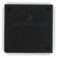
MMC2107CFCAG33
Manufacturer Part Number
MMC2107CFCAG33
Description
IC MCU 33MHZ 128K FLASH 144-LQFP
Manufacturer
Freescale Semiconductor
Series
MCorer
Datasheet
1.MMC2107CFCAF33.pdf
(618 pages)
Specifications of MMC2107CFCAG33
Core Processor
M210
Core Size
32-Bit
Speed
33MHz
Connectivity
EBI/EMI, SCI, SPI
Peripherals
POR, PWM, WDT
Number Of I /o
72
Program Memory Size
128KB (128K x 8)
Program Memory Type
FLASH
Ram Size
8K x 8
Voltage - Supply (vcc/vdd)
2.7 V ~ 3.6 V
Data Converters
A/D 8x10b
Oscillator Type
Internal
Operating Temperature
-40°C ~ 85°C
Package / Case
144-LQFP
Processor Series
MMC2107
Core
M-CORE
Data Bus Width
32 bit
Data Ram Size
8 KB
Interface Type
SCI/SPI
Maximum Clock Frequency
33 MHz
Number Of Programmable I/os
72
Number Of Timers
2
Operating Supply Voltage
0 V to 3.6 V
Maximum Operating Temperature
+ 85 C
Mounting Style
SMD/SMT
Minimum Operating Temperature
- 40 C
On-chip Adc
8-ch x 10-bit
Cpu Family
Mcore
Device Core
MCORE
Device Core Size
32b
Frequency (max)
33MHz
Total Internal Ram Size
8KB
# I/os (max)
72
Number Of Timers - General Purpose
2
Operating Supply Voltage (typ)
3.3/5V
Operating Supply Voltage (max)
3.6/5.5V
Operating Supply Voltage (min)
2.7/4.5V
Instruction Set Architecture
RISC
Operating Temp Range
-40C to 85C
Operating Temperature Classification
Industrial
Mounting
Surface Mount
Pin Count
144
Package Type
LQFP
Lead Free Status / RoHS Status
Lead free / RoHS Compliant
Eeprom Size
-
Lead Free Status / Rohs Status
Lead free / RoHS Compliant
Available stocks
Company
Part Number
Manufacturer
Quantity
Price
Company:

Part Number:
MMC2107CFCAG33
Manufacturer:
FREESCALE
Quantity:
210
Company:
Part Number:
MMC2107CFCAG33
Manufacturer:
freescaie
Quantity:
35
Company:
Part Number:
MMC2107CFCAG33
Manufacturer:
Freescale Semiconductor
Quantity:
10 000


21.14.12.4 Writeback Bus Register
21.14.12.5 Processor Status Register
MMC2107 – Rev. 2.0
MOTOROLA
TC — Prefetch Transfer Code
The writeback bus register (WBBR) is a means of passing operand
information between the CPU and the external command controller.
Whenever the external command controller needs to read the contents
of a register or memory location, it forces the device to execute an
instruction that brings that information to WBBR.
For example, to read the content of processor register r0, a MOV r0,r0
instruction is executed, and the result value of the instruction is latched
into the WBBR. The contents of WBBR can then be delivered serially to
the external command controller.
To update a processor resource, this register is initialized with a data
value to be written, and a MOV instruction is executed which uses this
value as a write-back data value. The FFY bit in the CTL register forces
the value of the WBBR to be substituted for the normal source value of
a MOV instruction, thus allowing updates to processor registers to be
performed.
The processor status register (PSR) is a 32-bit latch used to read or write
the M•CORE processor status register. Whenever the external
command controller needs to save or modify the contents of the
M•CORE processor status register, the PSR is used. This register is
affected by the operations performed in debug mode and must be
restored by the external command controller when returning to normal
mode.
This control field is used to drive the CPU TC2–TC0 outputs on the
first instruction pre-fetch caused by issuing a OnCE command with
the GO bit set and not ignored. It should typically be set to indicate a
supervisor instruction access, for example, 0b110. This field should
be restored to its original value after a debug session is completed,
for example, when a OnCE command is issued with the GO and EX
bits set and not ignored.
Freescale Semiconductor, Inc.
For More Information On This Product,
JTAG Test Access Port and OnCE
Go to: www.freescale.com
JTAG Test Access Port and OnCE
Functional Description
Technical Data
579
Related parts for MMC2107CFCAG33
Image
Part Number
Description
Manufacturer
Datasheet
Request
R

Part Number:
Description:
Manufacturer:
Freescale Semiconductor, Inc
Datasheet:
Part Number:
Description:
Manufacturer:
Freescale Semiconductor, Inc
Datasheet:
Part Number:
Description:
Manufacturer:
Freescale Semiconductor, Inc
Datasheet:
Part Number:
Description:
Manufacturer:
Freescale Semiconductor, Inc
Datasheet:
Part Number:
Description:
Manufacturer:
Freescale Semiconductor, Inc
Datasheet:
Part Number:
Description:
Manufacturer:
Freescale Semiconductor, Inc
Datasheet:
Part Number:
Description:
Manufacturer:
Freescale Semiconductor, Inc
Datasheet:
Part Number:
Description:
Manufacturer:
Freescale Semiconductor, Inc
Datasheet:
Part Number:
Description:
Manufacturer:
Freescale Semiconductor, Inc
Datasheet:
Part Number:
Description:
Manufacturer:
Freescale Semiconductor, Inc
Datasheet:
Part Number:
Description:
Manufacturer:
Freescale Semiconductor, Inc
Datasheet:
Part Number:
Description:
Manufacturer:
Freescale Semiconductor, Inc
Datasheet:
Part Number:
Description:
Manufacturer:
Freescale Semiconductor, Inc
Datasheet:
Part Number:
Description:
Manufacturer:
Freescale Semiconductor, Inc
Datasheet:
Part Number:
Description:
Manufacturer:
Freescale Semiconductor, Inc
Datasheet: