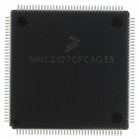
MMC2107CFCAG33 Freescale Semiconductor, MMC2107CFCAG33 Datasheet - Page 446

MMC2107CFCAG33
Manufacturer Part Number
MMC2107CFCAG33
Description
IC MCU 33MHZ 128K FLASH 144-LQFP
Manufacturer
Freescale Semiconductor
Series
MCorer
Datasheet
1.MMC2107CFCAF33.pdf
(618 pages)
Specifications of MMC2107CFCAG33
Core Processor
M210
Core Size
32-Bit
Speed
33MHz
Connectivity
EBI/EMI, SCI, SPI
Peripherals
POR, PWM, WDT
Number Of I /o
72
Program Memory Size
128KB (128K x 8)
Program Memory Type
FLASH
Ram Size
8K x 8
Voltage - Supply (vcc/vdd)
2.7 V ~ 3.6 V
Data Converters
A/D 8x10b
Oscillator Type
Internal
Operating Temperature
-40°C ~ 85°C
Package / Case
144-LQFP
Processor Series
MMC2107
Core
M-CORE
Data Bus Width
32 bit
Data Ram Size
8 KB
Interface Type
SCI/SPI
Maximum Clock Frequency
33 MHz
Number Of Programmable I/os
72
Number Of Timers
2
Operating Supply Voltage
0 V to 3.6 V
Maximum Operating Temperature
+ 85 C
Mounting Style
SMD/SMT
Minimum Operating Temperature
- 40 C
On-chip Adc
8-ch x 10-bit
Cpu Family
Mcore
Device Core
MCORE
Device Core Size
32b
Frequency (max)
33MHz
Total Internal Ram Size
8KB
# I/os (max)
72
Number Of Timers - General Purpose
2
Operating Supply Voltage (typ)
3.3/5V
Operating Supply Voltage (max)
3.6/5.5V
Operating Supply Voltage (min)
2.7/4.5V
Instruction Set Architecture
RISC
Operating Temp Range
-40C to 85C
Operating Temperature Classification
Industrial
Mounting
Surface Mount
Pin Count
144
Package Type
LQFP
Lead Free Status / RoHS Status
Lead free / RoHS Compliant
Eeprom Size
-
Lead Free Status / Rohs Status
Lead free / RoHS Compliant
Available stocks
Company
Part Number
Manufacturer
Quantity
Price
Company:
Part Number:
MMC2107CFCAG33
Manufacturer:
FREESCALE
Quantity:
210
Company:
Part Number:
MMC2107CFCAG33
Manufacturer:
freescaie
Quantity:
35
Company:
Part Number:
MMC2107CFCAG33
Manufacturer:
Freescale Semiconductor
Quantity:
10 000
- Current page: 446 of 618
- Download datasheet (8Mb)
Queued Analog-to-Digital Converter (QADC)
18.9.2.3 External Multiplexed Address Configuration
18.9.3 Analog Subsystem
18.9.3.1 Analog-to-Digital Converter Operation
18.9.3.2 Conversion Cycle Times
Technical Data
446
NOTE:
The QADC can drive external multiplexed addresses. If configured to
drive external addresses, the external address pins MA[1:0] will function
as address pins and will not maintain analog input functions in external
address mode.
This section describes the QADC analog subsystem, which includes the
front-end analog multiplexer and analog-to-digital converter.
The analog subsystem consists of the path from the input pins to the A/D
converter block. Signals from the queue control logic are fed to the
multiplexer and state machine. The end-of-conversion (EOC) signal and
the successive-approximation register (SAR) reflect the result of the
conversion.
subsystem.
The following description assumes the use of a buffer amplifier.
Total conversion time is made up of initial sample time, final sample time,
and resolution time. Initial sample time refers to the time during which the
selected input channel is coupled through the buffer amplifier to the
sample capacitor. This buffer is used to quickly reproduce its input signal
on the sample capacitor and minimize charge sharing errors. During the
final sampling period the amplifier is bypassed, and the multiplexer input
charges the sample capacitor array directly for improved accuracy.
During the resolution period, the voltage in the sample capacitor is
converted to a digital value and stored in the SAR.
Initial sample time is fixed at two QCLK cycles. Final sample time can be
2, 4, 8, or 16 QCLK cycles, depending on the value of the IST field in the
CCW. Resolution time is 10 QCLK cycles.
Freescale Semiconductor, Inc.
For More Information On This Product,
Queued Analog-to-Digital Converter (QADC)
Figure 18-19
Go to: www.freescale.com
shows a block diagram of the QADC analog
MMC2107 – Rev. 2.0
MOTOROLA
Related parts for MMC2107CFCAG33
Image
Part Number
Description
Manufacturer
Datasheet
Request
R
Part Number:
Description:
Manufacturer:
Freescale Semiconductor, Inc
Datasheet:
Part Number:
Description:
Manufacturer:
Freescale Semiconductor, Inc
Datasheet:
Part Number:
Description:
Manufacturer:
Freescale Semiconductor, Inc
Datasheet:
Part Number:
Description:
Manufacturer:
Freescale Semiconductor, Inc
Datasheet:
Part Number:
Description:
Manufacturer:
Freescale Semiconductor, Inc
Datasheet:
Part Number:
Description:
Manufacturer:
Freescale Semiconductor, Inc
Datasheet:
Part Number:
Description:
Manufacturer:
Freescale Semiconductor, Inc
Datasheet:
Part Number:
Description:
Manufacturer:
Freescale Semiconductor, Inc
Datasheet:
Part Number:
Description:
Manufacturer:
Freescale Semiconductor, Inc
Datasheet:
Part Number:
Description:
Manufacturer:
Freescale Semiconductor, Inc
Datasheet:
Part Number:
Description:
Manufacturer:
Freescale Semiconductor, Inc
Datasheet:
Part Number:
Description:
Manufacturer:
Freescale Semiconductor, Inc
Datasheet:
Part Number:
Description:
Manufacturer:
Freescale Semiconductor, Inc
Datasheet:
Part Number:
Description:
Manufacturer:
Freescale Semiconductor, Inc
Datasheet:
Part Number:
Description:
Manufacturer:
Freescale Semiconductor, Inc
Datasheet:


