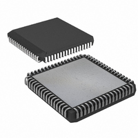
DS80C390-QCR+ Maxim Integrated Products, DS80C390-QCR+ Datasheet - Page 39

DS80C390-QCR+
Manufacturer Part Number
DS80C390-QCR+
Description
IC MPU CAN DUAL HS 68-PLCC
Manufacturer
Maxim Integrated Products
Series
80Cr
Datasheet
1.DS80C390-FCR.pdf
(53 pages)
Specifications of DS80C390-QCR+
Core Processor
8051
Core Size
8-Bit
Speed
40MHz
Connectivity
CAN, EBI/EMI, SIO, UART/USART
Peripherals
Power-Fail Reset, WDT
Number Of I /o
32
Program Memory Type
ROMless
Ram Size
4K x 8
Voltage - Supply (vcc/vdd)
3.85 V ~ 5.5 V
Oscillator Type
External
Operating Temperature
0°C ~ 70°C
Package / Case
68-LCC, 68-PLCC
Processor Series
DS80C390
Core
8051
Data Bus Width
8 bit
Program Memory Size
4 KB
Data Ram Size
4 KB
Interface Type
CAN, IrDA
Maximum Clock Frequency
40 MHz
Number Of Programmable I/os
32
Number Of Timers
3
Operating Supply Voltage
3.85 V to 5.5 V
Maximum Operating Temperature
+ 70 C
Mounting Style
SMD/SMT
3rd Party Development Tools
PK51, CA51, A51, ULINK2
Minimum Operating Temperature
0 C
Package
68PLCC
Device Core
8051
Family Name
80C
Maximum Speed
40 MHz
Lead Free Status / RoHS Status
Lead free / RoHS Compliant
Eeprom Size
-
Program Memory Size
-
Data Converters
-
Lead Free Status / Rohs Status
Details
the microcontroller can never be operated faster than 40MHz. This means that the maximum crystal oscillator or
external clock source is 10MHz when using the 4X setting, and 20MHz when using the 2X setting.
The primary advantage of the clock multiplier is that it allows the microcontroller to use slower crystals to achieve
the same performance level. This reduces EMI and cost, as slower crystals are generally more available and thus
less expensive.
Table 11. System Clock Configuration
The system clock and machine cycle rate changes one machine cycle after the instruction changing the control
bits. Note that the change affects all aspects of system operation, including timers and baud rates. The use of the
switchback feature, described later, can eliminate many of the problems associated with the PMM.
Changing the System Clock/Machine Cycle Clock Frequency
The microcontroller incorporates a special locking sequence to ensure “glitch-free” switching of the internal clock
signals. All changes to the CD1, CD0 bits must pass through the 10 (divide-by-4) state. For example, to change
from 00 (frequency multiplier) to 11 (PMM), the software must change the bits in the following sequence: 00 ≥ 10 ≥
11. Attempts to switch between invalid states will fail, leaving the CD1, CD0 bits unchanged.
The following sequence must be followed when switching to the frequency multiplier as the internal time source.
This sequence can only be performed when the device is in divide-by-4 operation. The steps must be followed in
this order, although it is possible to have other instructions between them. Any deviation from this order will cause
the CD1, CD0 bits to remain unchanged. Switching from frequency multiplier to non-multiplier mode requires no
steps other than the changing of the CD1, CD0 bits.
1) Ensure that the CD1, CD0 bits are set to 10, and the RGMD (EXIF.2) bit = 0.
2) Clear the CTM (Crystal Multiplier Enable) bit.
3) Set the 4X/2X bit to the appropriate state.
4) Set the CTM (crystal multiplier enable) bit.
5) Poll the CKRDY bit (EXIF.4), waiting until it is set to 1. This will take approximately 65,536 cycles of the
6) Set CD1, CD0 to 00. The frequency multiplier is engaged on the machine cycle following the write to these bits.
OSCILLATOR-FAIL DETECT
The microprocessor contains a safety mechanism called an on-chip oscillator-fail-detect circuit. When enabled, this
circuit causes the processor to be held in reset if the oscillator frequency falls below 40kHz. In operation, this circuit
complements the watchdog timer. Normally, the watchdog timer is initialized so that it times out and causes a
processor reset in the event that the processor loses control. In the event of a crystal or external oscillator failure,
however, the watchdog timer does not function and there is the potential for the processor to fail in an uncontrolled
state. The use of the oscillator-fail-detect circuit forces the processor to a known state (i.e., reset) even if the
oscillator stops.
The oscillator-fail-detect circuitry is enabled when software sets the enable bit OFDE (PCON.4) to 1. Please note
that software must use a timed-access procedure (described later) to write this bit. The OFDF (PCON.5) bit also
sets to 1 when the circuitry detects an oscillator failure, and the processor is forced into a reset state. This bit can
only be cleared to 0 by a power-fail reset or by software. The oscillator-fail-detect circuitry is not activated when the
oscillator is stopped due to the processor entering stop mode.
CD1
external crystal or clock source.
0
0
0
1
1
CD0
0
0
1
0
1
4X/2X
N/A
N/A
N/A
0
1
Power Management Mode
Frequency Multiplier (2X)
Frequency Multiplier (4X)
Divide-by-4 (Default)
FUNCTION
Reserved
39 of 53
MACHINE CYCLE
CLOCKS PER
1024
—
2
1
4
MAX EXTERNAL
FREQUENCY
(MHz)
20
10
40
40
—


