DS80C390-QCR+ Maxim Integrated Products, DS80C390-QCR+ Datasheet - Page 26
DS80C390-QCR+
Manufacturer Part Number
DS80C390-QCR+
Description
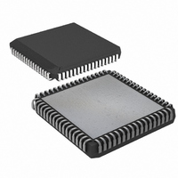
IC MPU CAN DUAL HS 68-PLCC
Manufacturer
Maxim Integrated Products
Series
80Cr
Datasheet
1.DS80C390-FCR.pdf
(53 pages)
Specifications of DS80C390-QCR+
Core Processor
8051
Core Size
8-Bit
Speed
40MHz
Connectivity
CAN, EBI/EMI, SIO, UART/USART
Peripherals
Power-Fail Reset, WDT
Number Of I /o
32
Program Memory Type
ROMless
Ram Size
4K x 8
Voltage - Supply (vcc/vdd)
3.85 V ~ 5.5 V
Oscillator Type
External
Operating Temperature
0°C ~ 70°C
Package / Case
68-LCC, 68-PLCC
Processor Series
DS80C390
Core
8051
Data Bus Width
8 bit
Program Memory Size
4 KB
Data Ram Size
4 KB
Interface Type
CAN, IrDA
Maximum Clock Frequency
40 MHz
Number Of Programmable I/os
32
Number Of Timers
3
Operating Supply Voltage
3.85 V to 5.5 V
Maximum Operating Temperature
+ 70 C
Mounting Style
SMD/SMT
3rd Party Development Tools
PK51, CA51, A51, ULINK2
Minimum Operating Temperature
0 C
Package
68PLCC
Device Core
8051
Family Name
80C
Maximum Speed
40 MHz
Lead Free Status / RoHS Status
Lead free / RoHS Compliant
Eeprom Size
-
Program Memory Size
-
Data Converters
-
Lead Free Status / Rohs Status
Details


PIN DESCRIPTION (continued)
58–64, 1
10–13
LQFP
4–7,
58
59
60
61
62
63
64
35
36
37
38
39
42
43
44
10
11
12
13
1
4
5
6
7
PIN
2–8, 10
13–16,
PLCC
19–22
10
46
47
48
49
50
53
54
55
13
14
15
16
19
20
21
22
2
3
4
5
6
7
8
A10 (P2.2)
A11 (P2.3)
A12 (P2.4)
A13 (P2.5)
A14 (P2.6)
A15 (P2.7)
P1.0–P1.7
P3.0–P3.7
A8 (P2.0)
A9 (P2.1)
NAME
A0
A1
A2
A3
A4
A5
A6
A7
Port 1, I/O. Port 1 can function as an 8-bit bidirectional I/O port, the
nonmultiplexed A0–A7 signals (when the MUX pin = 1), and as an
alternate interface for internal resources. Setting the SP1EC bit
relocates RXD1 and TXD1 to Port 5. The reset condition of Port 1 is
all bits at logic 1 through a weak pullup. The logic 1 state also serves
as an input mode, since external circuits writing to the port can
overdrive the weak pullup. When software clears any port pin to 0, a
strong pulldown is activated that remains on until either a 1 is written
to the port pin or a reset occurs. Writing a 1 after the port has been at
0 activates a strong transition driver, followed by a weaker sustaining
pullup. Once the momentary strong driver turns off, the port once
again becomes the output (and input) high state.
Port
P1.0
P1.1
P1.2
P1.3
P1.4
P1.5
P1.6
P1.7
A15–A8 (Port 2), Output. Port 2 serves as the MSB for external
addressing. The port automatically asserts the address MSB during
external ROM and RAM access. Although the Port 2 SFR exists, the
SFR value never appears on the pins (due to memory access).
Therefore, accessing the Port 2 SFR is only useful for MOVX A, @Ri
or MOVX @Ri, A instructions, which use the Port 2 SFR as the
external address MSB.
Port 3, I/O. Port 3 functions as an 8-bit bidirectional I/O port and as an
alternate interface for several resources found on the traditional 8051.
The reset condition of Port 1 is all bits at logic 1 through a weak pullup.
The logic 1 state also serves as an input mode, since external circuits
writing to the port can overdrive the weak pullup. When software clears
any port pin to 0, the device activates a strong pulldown that remains on
until either a 1 is written to the port pin or a reset occurs. Writing a 1 after
the port has been at 0 activates a strong transition driver, followed by a
weaker sustaining pullup. Once the momentary strong driver turns off,
the port once again becomes the output (and input) high state.
Port
P3.0
P3.1
P3.2
P3.3
P3.4
P3.5
P3.6
P3.7
Alternate Function
T2 External I/O for Timer/Counter 2
T2EX Timer/Counter 2 Capture/Reload Trigger
RXD1 Serial Port 1 Input
TXD1 Serial Port 1 Output
INT2 External Interrupt 2 (Positive Edge Detect)
INT3 External Interrupt 3 (Negative Edge Detect)
INT4 External Interrupt 4 (Positive Edge Detect)
INT5 External Interrupt 5 (Negative Edge Detect)
Alternate Function
RXD0 Serial Port 0 Input
TXD0 Serial Port 0 Output
INT0 External Interrupt 0
INT1 External Interrupt 1
T0 Timer 0 External Input
T1/XCLK Timer 1 External Input/External Clock Output
WR External Data Memory Write Strobe
RD External Data Memory Read Strobe
26 of 53
FUNCTION
Related parts for DS80C390-QCR+
Image
Part Number
Description
Manufacturer
Datasheet
Request
R

Part Number:
Description:
Manufacturer:
Maxim Integrated Products
Datasheet:

Part Number:
Description:
IC MPU CAN DUAL HS 64-LQFP
Manufacturer:
Maxim Integrated Products
Datasheet:
Part Number:
Description:
IC MPU CAN DUAL HS IND 64-LQFP
Manufacturer:
Maxim Integrated Products
Datasheet:

Part Number:
Description:
IC MPU CAN DUAL HS 68-PLCC
Manufacturer:
Maxim Integrated Products
Datasheet:
Part Number:
Description:
IC MPU CAN DUAL HS IND 68-PLCC
Manufacturer:
Maxim Integrated Products
Datasheet:
Part Number:
Description:
IC MPU CAN DUAL HS IND 68-PLCC
Manufacturer:
Maxim Integrated Products
Datasheet:
Part Number:
Description:
IC MPU CAN DUAL HS 64-LQFP
Manufacturer:
Maxim Integrated Products
Datasheet:
Part Number:
Description:
IC MPU CAN DUAL HS IND 64-LQFP
Manufacturer:
Maxim Integrated Products
Datasheet:
Part Number:
Description:
MAX7528KCWPMaxim Integrated Products [CMOS Dual 8-Bit Buffered Multiplying DACs]
Manufacturer:
Maxim Integrated Products
Datasheet:
Part Number:
Description:
Single +5V, fully integrated, 1.25Gbps laser diode driver.
Manufacturer:
Maxim Integrated Products
Datasheet:
Part Number:
Description:
Single +5V, fully integrated, 155Mbps laser diode driver.
Manufacturer:
Maxim Integrated Products
Datasheet:
Part Number:
Description:
VRD11/VRD10, K8 Rev F 2/3/4-Phase PWM Controllers with Integrated Dual MOSFET Drivers
Manufacturer:
Maxim Integrated Products
Datasheet:
Part Number:
Description:
Highly Integrated Level 2 SMBus Battery Chargers
Manufacturer:
Maxim Integrated Products
Datasheet:
Part Number:
Description:
Current Monitor and Accumulator with Integrated Sense Resistor; ; Temperature Range: -40°C to +85°C
Manufacturer:
Maxim Integrated Products
Part Number:
Description:
TSSOP 14/A°/RS-485 Transceivers with Integrated 100O/120O Termination Resis
Manufacturer:
Maxim Integrated Products