DS80C390-QCR+ Maxim Integrated Products, DS80C390-QCR+ Datasheet - Page 38
DS80C390-QCR+
Manufacturer Part Number
DS80C390-QCR+
Description
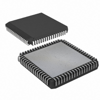
IC MPU CAN DUAL HS 68-PLCC
Manufacturer
Maxim Integrated Products
Series
80Cr
Datasheet
1.DS80C390-FCR.pdf
(53 pages)
Specifications of DS80C390-QCR+
Core Processor
8051
Core Size
8-Bit
Speed
40MHz
Connectivity
CAN, EBI/EMI, SIO, UART/USART
Peripherals
Power-Fail Reset, WDT
Number Of I /o
32
Program Memory Type
ROMless
Ram Size
4K x 8
Voltage - Supply (vcc/vdd)
3.85 V ~ 5.5 V
Oscillator Type
External
Operating Temperature
0°C ~ 70°C
Package / Case
68-LCC, 68-PLCC
Processor Series
DS80C390
Core
8051
Data Bus Width
8 bit
Program Memory Size
4 KB
Data Ram Size
4 KB
Interface Type
CAN, IrDA
Maximum Clock Frequency
40 MHz
Number Of Programmable I/os
32
Number Of Timers
3
Operating Supply Voltage
3.85 V to 5.5 V
Maximum Operating Temperature
+ 70 C
Mounting Style
SMD/SMT
3rd Party Development Tools
PK51, CA51, A51, ULINK2
Minimum Operating Temperature
0 C
Package
68PLCC
Device Core
8051
Family Name
80C
Maximum Speed
40 MHz
Lead Free Status / RoHS Status
Lead free / RoHS Compliant
Eeprom Size
-
Program Memory Size
-
Data Converters
-
Lead Free Status / Rohs Status
Details


INC DPTR
MOV DPTR, #data16
MOVC A, @A+DPTR
MOVX A, @DPTR
MOVX @DPTR, A
As a brief example, if TSL is set to 1, then both data pointers can be updated with two INC DPTR instructions.
Assume that SEL = 0, making DPTR the active data pointer. The first INC DPTR increments DPTR and toggles
SEL to 1. The second instruction increments DPTR1 and toggles SEL back to 0.
INC DPTR
INC DPTR
CLOCK CONTROL AND POWER MANAGEMENT
The DS80C390 includes a number of unique features that allow flexibility in selecting system clock sources and
operating frequencies. To support the use of inexpensive crystals while allowing full speed operation, a clock
multiplier is included in the processor’s clock circuit. Also, in addition to the standard 80C32 idle and power-down
(Stop) modes, the DS80C390 provides a new power management mode. This mode allows the processor to
continue instruction execution, yet at a very low speed to significantly reduce power consumption (below even idle
mode). The DS80C390 also features several enhancements to stop mode that make this extremely low-power
mode more useful. Each of these features is discussed in detail below.
System Clock Control
As mentioned previously, the microcontroller contains special clock-control circuitry that simultaneously provides
maximum timing flexibility and maximum availability and economy in crystal selection. The logical operation of the
system clock-divide control function is shown in
selects one of three sources for the internal system clock:
Figure 29. System Clock Control Diagram
The system clock-control circuitry generates two clock signals that are used by the microcontroller. The internal
system clock provides the time base for timers and internal peripherals. The system clock is run through a divide-
by-4 circuit to generate the machine cycle clock that provides the time base for CPU operations. All instructions
execute in one to five machine cycles. It is important to note the distinction between these two clock signals, as
they are sometimes confused, creating errors in timing calculations.
Setting CD1, CD0 to 0 enables the frequency multiplier, either doubling or quadrupling the frequency of the crystal
oscillator or external clock source. The 4X/2X bit controls the multiplying factor, selecting twice or four times the
frequency when set to 0 or 1, respectively. Enabling the frequency multiplier results in apparent instruction
execution speeds of 2 or 1 clocks. Regardless of the configuration of the frequency multiplier, the system clock of
Crystal oscillator or external clock source
(Crystal oscillator or external clock source) divided by 256
(Crystal oscillator or external clock source) frequency multiplied by 2 or 4 times
Figure
38 of 53
29. A 3:1 multiplexer, controlled by CD1, CD0 (PMR.7-6),
Related parts for DS80C390-QCR+
Image
Part Number
Description
Manufacturer
Datasheet
Request
R

Part Number:
Description:
Manufacturer:
Maxim Integrated Products
Datasheet:

Part Number:
Description:
IC MPU CAN DUAL HS 64-LQFP
Manufacturer:
Maxim Integrated Products
Datasheet:
Part Number:
Description:
IC MPU CAN DUAL HS IND 64-LQFP
Manufacturer:
Maxim Integrated Products
Datasheet:

Part Number:
Description:
IC MPU CAN DUAL HS 68-PLCC
Manufacturer:
Maxim Integrated Products
Datasheet:
Part Number:
Description:
IC MPU CAN DUAL HS IND 68-PLCC
Manufacturer:
Maxim Integrated Products
Datasheet:
Part Number:
Description:
IC MPU CAN DUAL HS IND 68-PLCC
Manufacturer:
Maxim Integrated Products
Datasheet:
Part Number:
Description:
IC MPU CAN DUAL HS 64-LQFP
Manufacturer:
Maxim Integrated Products
Datasheet:
Part Number:
Description:
IC MPU CAN DUAL HS IND 64-LQFP
Manufacturer:
Maxim Integrated Products
Datasheet:
Part Number:
Description:
MAX7528KCWPMaxim Integrated Products [CMOS Dual 8-Bit Buffered Multiplying DACs]
Manufacturer:
Maxim Integrated Products
Datasheet:
Part Number:
Description:
Single +5V, fully integrated, 1.25Gbps laser diode driver.
Manufacturer:
Maxim Integrated Products
Datasheet:
Part Number:
Description:
Single +5V, fully integrated, 155Mbps laser diode driver.
Manufacturer:
Maxim Integrated Products
Datasheet:
Part Number:
Description:
VRD11/VRD10, K8 Rev F 2/3/4-Phase PWM Controllers with Integrated Dual MOSFET Drivers
Manufacturer:
Maxim Integrated Products
Datasheet:
Part Number:
Description:
Highly Integrated Level 2 SMBus Battery Chargers
Manufacturer:
Maxim Integrated Products
Datasheet:
Part Number:
Description:
Current Monitor and Accumulator with Integrated Sense Resistor; ; Temperature Range: -40°C to +85°C
Manufacturer:
Maxim Integrated Products
Part Number:
Description:
TSSOP 14/A°/RS-485 Transceivers with Integrated 100O/120O Termination Resis
Manufacturer:
Maxim Integrated Products