DS80C390-QCR+ Maxim Integrated Products, DS80C390-QCR+ Datasheet - Page 25

DS80C390-QCR+
Manufacturer Part Number
DS80C390-QCR+
Description
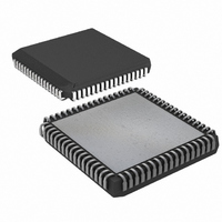
IC MPU CAN DUAL HS 68-PLCC
Manufacturer
Maxim Integrated Products
Series
80Cr
Datasheet
1.DS80C390-FCR.pdf
(53 pages)
Specifications of DS80C390-QCR+
Core Processor
8051
Core Size
8-Bit
Speed
40MHz
Connectivity
CAN, EBI/EMI, SIO, UART/USART
Peripherals
Power-Fail Reset, WDT
Number Of I /o
32
Program Memory Type
ROMless
Ram Size
4K x 8
Voltage - Supply (vcc/vdd)
3.85 V ~ 5.5 V
Oscillator Type
External
Operating Temperature
0°C ~ 70°C
Package / Case
68-LCC, 68-PLCC
Processor Series
DS80C390
Core
8051
Data Bus Width
8 bit
Program Memory Size
4 KB
Data Ram Size
4 KB
Interface Type
CAN, IrDA
Maximum Clock Frequency
40 MHz
Number Of Programmable I/os
32
Number Of Timers
3
Operating Supply Voltage
3.85 V to 5.5 V
Maximum Operating Temperature
+ 70 C
Mounting Style
SMD/SMT
3rd Party Development Tools
PK51, CA51, A51, ULINK2
Minimum Operating Temperature
0 C
Package
68PLCC
Device Core
8051
Family Name
80C
Maximum Speed
40 MHz
Lead Free Status / RoHS Status
Lead free / RoHS Compliant
Eeprom Size
-
Program Memory Size
-
Data Converters
-
Lead Free Status / Rohs Status
Details
PIN DESCRIPTION
8, 22, 40,
9, 25, 41,
LQFP
56
57
46
45
47
26
23
24
55
54
53
52
51
50
49
48
2
3
PIN
17, 32, 51,
1, 18, 35,
PLCC
68
52
57
56
58
36
11
12
33
34
67
66
65
64
63
62
61
59
AD0/D0
AD1/D1
AD2/D2
AD3/D3
AD4/D4
AD5/D5
AD6/D6
AD7/D7
RSTOL
XTAL2
XTAL1
NAME
PSEN
GND
MUX
RST
ALE
V
EA
CC
+5V
Digital Circuit Ground
Address Latch Enable, Output. When the MUX pin is low, this pin
outputs a clock to latch the external address LSB from the
multiplexed address/data bus on Port 0. This signal is commonly
connected to the latch enable of an external transparent latch. ALE
has a pulse width of 1.5 XTAL1 cycles and a period of four XTAL1
cycles. When the MUX pin is high, the pin will toggle continuously if
the ALEOFF bit is cleared. ALE is forced high when the device is in a
reset condition or if the ALEOFF bit is set while the MUX pin is high.
Program Store Enable, Output. This signal is the chip enable for
external ROM memory. PSEN provides an active-low pulse and is
driven high when external ROM is not being accessed.
External Access Enable, Input. This pin must be wired to GND for
proper operation.
Multiplex/Demultiplex Select, Input. This pin selects if the
address/data bus operates in multiplexed (MUX = 0) or demultiplexed
(MUX = 1) mode.
Reset, Input. The RST input pin contains a Schmitt voltage input to
recognize external active-high reset inputs. The pin also employs an
internal pulldown resistor to allow for a combination of wired-OR
external reset sources. An RC circuit is not required for power-up, as
the device provides this function internally.
Reset Output Low, Output. This active-low signal is asserted:
When the processor has entered reset through the RST pin,
During crystal warmup period following power-on or stop mode,
During a watchdog timer reset (2 cycles duration),
During an oscillator failure (if OFDE = 1),
Whenever V
XTAL1, XTAL2. Crystal oscillator pins support fundamental mode,
parallel resonant, and AT-cut crystals. XTAL1 is the input if an
external clock source is used in place of a crystal. XTAL2 is the
output of the crystal amplifier.
AD0–7 (Port 0), I/O. When the MUX pin is wired low, Port 0 is the
multiplexed address/data bus. While ALE is high, the LSB of a
memory address is presented. While ALE falls, the port transitions to
a bidirectional data bus. When the MUX pin is wired high, Port 0
functions as the bidirectional data bus. Port 0 cannot be modified by
software. The reset condition of Port 0 pins is high. No pullup
resistors are needed.
25 of 53
CC
≤ V
RST.
FUNCTION


