DS80C390-QCR+ Maxim Integrated Products, DS80C390-QCR+ Datasheet - Page 2
DS80C390-QCR+
Manufacturer Part Number
DS80C390-QCR+
Description
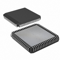
IC MPU CAN DUAL HS 68-PLCC
Manufacturer
Maxim Integrated Products
Series
80Cr
Datasheet
1.DS80C390-FCR.pdf
(53 pages)
Specifications of DS80C390-QCR+
Core Processor
8051
Core Size
8-Bit
Speed
40MHz
Connectivity
CAN, EBI/EMI, SIO, UART/USART
Peripherals
Power-Fail Reset, WDT
Number Of I /o
32
Program Memory Type
ROMless
Ram Size
4K x 8
Voltage - Supply (vcc/vdd)
3.85 V ~ 5.5 V
Oscillator Type
External
Operating Temperature
0°C ~ 70°C
Package / Case
68-LCC, 68-PLCC
Processor Series
DS80C390
Core
8051
Data Bus Width
8 bit
Program Memory Size
4 KB
Data Ram Size
4 KB
Interface Type
CAN, IrDA
Maximum Clock Frequency
40 MHz
Number Of Programmable I/os
32
Number Of Timers
3
Operating Supply Voltage
3.85 V to 5.5 V
Maximum Operating Temperature
+ 70 C
Mounting Style
SMD/SMT
3rd Party Development Tools
PK51, CA51, A51, ULINK2
Minimum Operating Temperature
0 C
Package
68PLCC
Device Core
8051
Family Name
80C
Maximum Speed
40 MHz
Lead Free Status / RoHS Status
Lead free / RoHS Compliant
Eeprom Size
-
Program Memory Size
-
Data Converters
-
Lead Free Status / Rohs Status
Details


Note 1:
Note 2:
Note 3:
Note 4:
Note 5:
Note 6:
Note 7:
Note 8:
Note 9:
Note 10:
ABSOLUTE MAXIMUM RATINGS
Voltage Range on Any Pin Relative to Ground……………………………………………………….-0.3V to (V
Voltage Range on V
Operating Temperature Range………………………………………………………………………………..-40°C to +85°C
Storage Temperature Range………………………………………………………………………………...-55°C to +125°C
Soldering Temperature…..……………………………………………………………………..See IPC/JEDEC J-STD-020
Stresses beyond those listed under “Absolute Maximum Ratings” may cause permanent damage to the device. These are stress ratings only,
and functional operation of the device at these or any other conditions beyond those indicated in the operational sections of the specifications is
not implied. Exposure to the absolute maximum rating conditions for extended periods may affect device reliability.
DC ELECTRICAL CHARACTERISTICS (Note 10)
Supply Voltage
Power-Fail Warning
Minimum Operating Voltage
Supply Current, Active Mode (Note 1)
Supply Current, Idle Mode (Note 2)
Supply Current, Stop Mode (Note 3)
Supply Current, Stop Mode, Bandgap Enabled (Note 3)
Input Low Level
Input High Level
Input High Level for XTAL1, RST
Output Low Voltage for Port 1, 3, 4, 5 at I
Output Low Voltage for Port 0, 1, 2, 4, 5, RD, WR, RSTOL, PSEN,
and ALE at I
Output High Voltage for Port 1, 3, 4, 5 at I
Output High Voltage for Port 1, 3, 4, 5 at I
Output High Voltage for Port 0, 1, 2, 4, 5, RD, WR, RSTOL, PSEN,
and ALE at I
Input Low Current for Port 1, 3, 4, 5 at 0.45V (Note 8)
Logic 1 to 0 Transition Current for Port 1, 3, 4, 5 (Note 9)
Input Leakage Current for Port 0 (Input Mode Only)
RST Pulldown Resistance
Active current measured with 40MHz clock source on XTAL1, V
Idle mode current measured with 40MHz clock source on XTAL1, V
Stop mode current measured with XTAL1 = RST = EA = V
RST = V
Applies to port pins when they are used to address external memory or as CAN interface signals.
This measurement reflects the port during a 0-to-1 transition in I/O mode. During this period a one-shot circuit drives the ports hard
for two clock cycles. If a port 4 or 5 pin is functioning in memory mode with pin state of 0 and the SFR bit contains a 1, changing
the pin to an I/O mode (by writing to P4CNT) will not enable the 2-cycle strong pullup. During Stop or Idle mode the pins switch to
I/O mode, and so port 2 and port 1 (in nonmultiplexed mode) will not exhibit the 2-cycle strong pullup when entering Stop or Idle
mode.
Port 3 pins 3.6 and 3.7 have a stronger than normal pullup drive for one oscillator period following the transition of either the RD or
WR from a 0-to-1 transition.
This is the current required from an external circuit to hold a logic low level on an I/O pin while the corresponding port latch bit is
set to 1. This is only the current required to hold the low level; transitions from 1 to 0 on an I/O pin also have to overcome the
transition current.
Ports 1(in I/O mode), 3, 4, and 5 source transition current when being pulled down externally. It reaches its maximum at
approximately 2V.
Specifications to -40°C are guaranteed by design and not production tested.
OL
OH
= 3.2mA (Note 5)
= -8mA (Note 5, 7)
CC
. This condition mimics operation of pins in I/O mode.
CC
Relative to Ground……………………………………………………………………-0.3V to +6.0V
PARAMETER
OL
OH
OH
= 1.6mA
= -50μA (Note 4)
= -1.5mA (Note 6)
2 of 53
SS
, V
CC
CC
= 5.5V, all other pins disconnected.
SYMBOL
= RST = 5.5V, all other pins disconnected.
CC
V
I
I
R
V
V
V
V
V
V
I
V
V
STOP
SPBG
= 5.5V, RST = EA = V
V
I
IDLE
V
I
PFW
I
RST
CC
OH1
OH2
OH3
OL1
OL2
I
RST
T1
CC
IH2
IL
L
IH
IL
0.7 x V
V
-300
MIN
4.10
3.85
-0.5
2.0
2.4
2.4
2.4
50
RST
CC
SS
, all other pins disconnected.
TYP
4.38
4.13
150
5.0
80
40
1
V
V
CC
CC
+300
MAX
-650
4.60
4.35
+0.8
0.45
0.45
150
120
350
170
5.5
-55
75
+0.5
+0.5
CC
+ 0.5V)
UNITS
mA
mA
μA
μA
μA
μA
μA
kΩ
V
V
V
V
V
V
V
V
V
V
V
Related parts for DS80C390-QCR+
Image
Part Number
Description
Manufacturer
Datasheet
Request
R

Part Number:
Description:
Manufacturer:
Maxim Integrated Products
Datasheet:

Part Number:
Description:
IC MPU CAN DUAL HS 64-LQFP
Manufacturer:
Maxim Integrated Products
Datasheet:
Part Number:
Description:
IC MPU CAN DUAL HS IND 64-LQFP
Manufacturer:
Maxim Integrated Products
Datasheet:

Part Number:
Description:
IC MPU CAN DUAL HS 68-PLCC
Manufacturer:
Maxim Integrated Products
Datasheet:
Part Number:
Description:
IC MPU CAN DUAL HS IND 68-PLCC
Manufacturer:
Maxim Integrated Products
Datasheet:
Part Number:
Description:
IC MPU CAN DUAL HS IND 68-PLCC
Manufacturer:
Maxim Integrated Products
Datasheet:
Part Number:
Description:
IC MPU CAN DUAL HS 64-LQFP
Manufacturer:
Maxim Integrated Products
Datasheet:
Part Number:
Description:
IC MPU CAN DUAL HS IND 64-LQFP
Manufacturer:
Maxim Integrated Products
Datasheet:
Part Number:
Description:
MAX7528KCWPMaxim Integrated Products [CMOS Dual 8-Bit Buffered Multiplying DACs]
Manufacturer:
Maxim Integrated Products
Datasheet:
Part Number:
Description:
Single +5V, fully integrated, 1.25Gbps laser diode driver.
Manufacturer:
Maxim Integrated Products
Datasheet:
Part Number:
Description:
Single +5V, fully integrated, 155Mbps laser diode driver.
Manufacturer:
Maxim Integrated Products
Datasheet:
Part Number:
Description:
VRD11/VRD10, K8 Rev F 2/3/4-Phase PWM Controllers with Integrated Dual MOSFET Drivers
Manufacturer:
Maxim Integrated Products
Datasheet:
Part Number:
Description:
Highly Integrated Level 2 SMBus Battery Chargers
Manufacturer:
Maxim Integrated Products
Datasheet:
Part Number:
Description:
Current Monitor and Accumulator with Integrated Sense Resistor; ; Temperature Range: -40°C to +85°C
Manufacturer:
Maxim Integrated Products
Part Number:
Description:
TSSOP 14/A°/RS-485 Transceivers with Integrated 100O/120O Termination Resis
Manufacturer:
Maxim Integrated Products