DS80C390-QCR+ Maxim Integrated Products, DS80C390-QCR+ Datasheet - Page 35
DS80C390-QCR+
Manufacturer Part Number
DS80C390-QCR+
Description
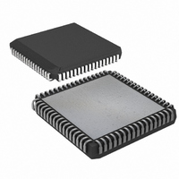
IC MPU CAN DUAL HS 68-PLCC
Manufacturer
Maxim Integrated Products
Series
80Cr
Datasheet
1.DS80C390-FCR.pdf
(53 pages)
Specifications of DS80C390-QCR+
Core Processor
8051
Core Size
8-Bit
Speed
40MHz
Connectivity
CAN, EBI/EMI, SIO, UART/USART
Peripherals
Power-Fail Reset, WDT
Number Of I /o
32
Program Memory Type
ROMless
Ram Size
4K x 8
Voltage - Supply (vcc/vdd)
3.85 V ~ 5.5 V
Oscillator Type
External
Operating Temperature
0°C ~ 70°C
Package / Case
68-LCC, 68-PLCC
Processor Series
DS80C390
Core
8051
Data Bus Width
8 bit
Program Memory Size
4 KB
Data Ram Size
4 KB
Interface Type
CAN, IrDA
Maximum Clock Frequency
40 MHz
Number Of Programmable I/os
32
Number Of Timers
3
Operating Supply Voltage
3.85 V to 5.5 V
Maximum Operating Temperature
+ 70 C
Mounting Style
SMD/SMT
3rd Party Development Tools
PK51, CA51, A51, ULINK2
Minimum Operating Temperature
0 C
Package
68PLCC
Device Core
8051
Family Name
80C
Maximum Speed
40 MHz
Lead Free Status / RoHS Status
Lead free / RoHS Compliant
Eeprom Size
-
Program Memory Size
-
Data Converters
-
Lead Free Status / Rohs Status
Details


INTERNAL MOVX SRAM
The DS80C390 contains 4kB of SRAM that can be configured as user accessible MOVX memory, program
memory, or optional stack memory. The specific configuration and locations are governed by the internal data
memory configuration bits (IDM1, IDM0) in the memory control register (MCON;C6h). Note that when the SA bit
(ACON.2) is set, the first 1kB of the MOVX data memory is reserved for use by the 10-bit expanded stack. Internal
memory accesses will not generate WR, RD, or PSEN strobes.
The DS80C390 can configure its 4kB of internal SRAM as combined program and data memory. This allows the
application software to execute self-modifiable code. The technique loads the 4kB SRAM with bootstrap loader
software, and then modifies the IDM1 and IDM0 bits to map the 4kB starting at memory location 40000h. This
allows the system to run the bootstrap loader without disturbing the 4MB external memory bus, making the device
in-system reprogrammable for flash or NV RAM.
Table 5. Internal MOVX SRAM Configuration
*10-bit expanded stack is not available in shared program/data memory mode.
EXTERNAL MEMORY ADDRESSING
The enabling and mapping of the chip-enable signals is done through the Port 4 control register (P4CNT;92h) and
memory control register (MCON; 96h).
Port 4. Following reset, the device will be configured with P4.7–P4.4 as address lines and P4.3–P4.0 configured as
CE3-0, with the first program fetch being performed from 00000h with CE0 active. The following tables illustrate
which memory ranges are controlled by each chip enable as a function of which address lines are enabled.
Table 6. External Memory Addressing Pin Assignments
Table 7. Extended Address and Chip-Enable Generation
IDM1
ADDRESS/DATA
111(default)
P4CNT.5–3
0
0
0
0
1
1
1
1
Demultiplexed
Multiplexed
000
100
101
110
BUS
IDM0
0
0
1
1
0
0
1
1
CMA
P4.7
A19
1
1
1
1
I/O
I/O
I/O
I/O
0
0
0
0
P4.3–P4.0
P4.3–P4.0
PORT 4 PIN FUNCTION
CE3–CE0
P4.6
A18
A18
I/O
I/O
I/O
00F000h–00FFFFh
00F000h–00FFFFh
000000h–000FFFh
000000h–000FFFh
400000h–400FFFh
400000h–400FFFh
MOVX DATA
—
—
P4.5
A17
A17
A17
I/O
I/O
Table 7
PCE3–PCE0
P5.7–P5.4
P5.7–P5.4
shows which chip-enable and address line signals are active on
P4.4
A16
A16
A16
A16
I/O
35 of 53
ADDR 19–16
P4.7–P4.4
P4.7–P4.4
P4CNT.2–0
111(default)
00EE00h–00EFFFh
00EE00h–00EFFFh
00EE00h–00EFFFh
00EE00h–00EFFFh
401000h–4011FFh
401000h–4011FFh
401000h–4011FFh
401000h–4011FFh
CAN MESSAGE
000
100
101
110
MEMORY
ADDR 15–8
P4.3
CE3
P2
P2
I/O
I/O
I/O
I/O
PORT 4 PIN FUNCTION
P4.2
CE2
CE2
SHARED PROGRAM/DATA
I/O
I/O
I/O
ADDR 7–0
400000h–400FFFh*
400000h–400FFFh*
P0
P1
P4.1
CE1
CE1
CE1
I/O
I/O
—
—
—
—
—
—
DATA BUS
P0
P0
P4.0
CE0
CE0
CE0
CE0
I/O
Related parts for DS80C390-QCR+
Image
Part Number
Description
Manufacturer
Datasheet
Request
R

Part Number:
Description:
Manufacturer:
Maxim Integrated Products
Datasheet:

Part Number:
Description:
IC MPU CAN DUAL HS 64-LQFP
Manufacturer:
Maxim Integrated Products
Datasheet:
Part Number:
Description:
IC MPU CAN DUAL HS IND 64-LQFP
Manufacturer:
Maxim Integrated Products
Datasheet:

Part Number:
Description:
IC MPU CAN DUAL HS 68-PLCC
Manufacturer:
Maxim Integrated Products
Datasheet:
Part Number:
Description:
IC MPU CAN DUAL HS IND 68-PLCC
Manufacturer:
Maxim Integrated Products
Datasheet:
Part Number:
Description:
IC MPU CAN DUAL HS IND 68-PLCC
Manufacturer:
Maxim Integrated Products
Datasheet:
Part Number:
Description:
IC MPU CAN DUAL HS 64-LQFP
Manufacturer:
Maxim Integrated Products
Datasheet:
Part Number:
Description:
IC MPU CAN DUAL HS IND 64-LQFP
Manufacturer:
Maxim Integrated Products
Datasheet:
Part Number:
Description:
MAX7528KCWPMaxim Integrated Products [CMOS Dual 8-Bit Buffered Multiplying DACs]
Manufacturer:
Maxim Integrated Products
Datasheet:
Part Number:
Description:
Single +5V, fully integrated, 1.25Gbps laser diode driver.
Manufacturer:
Maxim Integrated Products
Datasheet:
Part Number:
Description:
Single +5V, fully integrated, 155Mbps laser diode driver.
Manufacturer:
Maxim Integrated Products
Datasheet:
Part Number:
Description:
VRD11/VRD10, K8 Rev F 2/3/4-Phase PWM Controllers with Integrated Dual MOSFET Drivers
Manufacturer:
Maxim Integrated Products
Datasheet:
Part Number:
Description:
Highly Integrated Level 2 SMBus Battery Chargers
Manufacturer:
Maxim Integrated Products
Datasheet:
Part Number:
Description:
Current Monitor and Accumulator with Integrated Sense Resistor; ; Temperature Range: -40°C to +85°C
Manufacturer:
Maxim Integrated Products
Part Number:
Description:
TSSOP 14/A°/RS-485 Transceivers with Integrated 100O/120O Termination Resis
Manufacturer:
Maxim Integrated Products