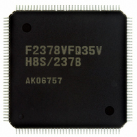
DF2378BVFQ35WV Renesas Electronics America, DF2378BVFQ35WV Datasheet - Page 839

DF2378BVFQ35WV
Manufacturer Part Number
DF2378BVFQ35WV
Description
IC H8S/2378 MCU FLASH 144-QFP
Manufacturer
Renesas Electronics America
Series
H8® H8S/2300r
Datasheet
1.YR0K42378FC000BA.pdf
(1208 pages)
Specifications of DF2378BVFQ35WV
Core Processor
H8S/2000
Core Size
16-Bit
Speed
35MHz
Connectivity
I²C, IrDA, SCI, SmartCard
Peripherals
DMA, POR, PWM, WDT
Number Of I /o
97
Program Memory Size
512KB (512K x 8)
Program Memory Type
FLASH
Ram Size
32K x 8
Voltage - Supply (vcc/vdd)
3 V ~ 3.6 V
Data Converters
A/D 16x10b; D/A 6x8b
Oscillator Type
Internal
Operating Temperature
-40°C ~ 85°C
Package / Case
144-QFP
For Use With
EDK2378 - DEV EVAL KIT FOR H8S/2378
Lead Free Status / RoHS Status
Lead free / RoHS Compliant
Eeprom Size
-
Available stocks
Company
Part Number
Manufacturer
Quantity
Price
Company:
Part Number:
DF2378BVFQ35WV
Manufacturer:
Renesas Electronics America
Quantity:
10 000
- Current page: 839 of 1208
- Download datasheet (8Mb)
An I
item:
1. For the masked ROM version, W is added to the model name of the product that uses optional
This LSI has a two-channel I
The I
(inter-IC bus) interface (Rev. 03) standard and fast mode functions. The register configuration that
controls the I
Figure 16.1 shows a block diagram of the I
Figure 16.2 shows an example of I/O pin connections to external circuits.
16.1
• Continuous transmission/reception
• Start and stop conditions generated automatically in master mode
• Selection of acknowledge output levels when receiving
• Automatic loading of acknowledge bit when transmitting
• Bit synchronization/wait function
• Six interrupt sources
• Direct bus drive
IFIIC40A_010020020400
functions.
For example: HD6432375WFQ
Since the shift register, transmit data register, and receive data register are independent from
each other, the continuous transmission/reception can be performed.
In master mode, the state of SCL is monitored per bit, and the timing is synchronized
automatically
If transmission/reception is not yet possible, set the SCL to low until preparations are
completed.
Transmit-data-empty (including slave-address match), transmit-end, receive-data-full
(including slave-address match), arbitration lost, NACK detection, and stop condition
detection
Two pins, SCL and SDA pins function as NMOS open-drain outputs.
2
C bus interface is an option. When using the optional functions, take notice of the following
2
C bus interface conforms to and provides a subset of the NXP Semiconductors I
Features
Section 16 I
2
C bus differs partly from the NXP Semiconductors configuration, however.
2
C bus interface.
2
C Bus Interface 2 (IIC2) (Option)
2
C bus interface 2.
Section 16 I
Rev.7.00 Mar. 18, 2009 page 771 of 1136
2
C Bus Interface 2 (IIC2) (Option)
REJ09B0109-0700
2
C bus
Related parts for DF2378BVFQ35WV
Image
Part Number
Description
Manufacturer
Datasheet
Request
R

Part Number:
Description:
KIT STARTER FOR M16C/29
Manufacturer:
Renesas Electronics America
Datasheet:

Part Number:
Description:
KIT STARTER FOR R8C/2D
Manufacturer:
Renesas Electronics America
Datasheet:

Part Number:
Description:
R0K33062P STARTER KIT
Manufacturer:
Renesas Electronics America
Datasheet:

Part Number:
Description:
KIT STARTER FOR R8C/23 E8A
Manufacturer:
Renesas Electronics America
Datasheet:

Part Number:
Description:
KIT STARTER FOR R8C/25
Manufacturer:
Renesas Electronics America
Datasheet:

Part Number:
Description:
KIT STARTER H8S2456 SHARPE DSPLY
Manufacturer:
Renesas Electronics America
Datasheet:

Part Number:
Description:
KIT STARTER FOR R8C38C
Manufacturer:
Renesas Electronics America
Datasheet:

Part Number:
Description:
KIT STARTER FOR R8C35C
Manufacturer:
Renesas Electronics America
Datasheet:

Part Number:
Description:
KIT STARTER FOR R8CL3AC+LCD APPS
Manufacturer:
Renesas Electronics America
Datasheet:

Part Number:
Description:
KIT STARTER FOR RX610
Manufacturer:
Renesas Electronics America
Datasheet:

Part Number:
Description:
KIT STARTER FOR R32C/118
Manufacturer:
Renesas Electronics America
Datasheet:

Part Number:
Description:
KIT DEV RSK-R8C/26-29
Manufacturer:
Renesas Electronics America
Datasheet:

Part Number:
Description:
KIT STARTER FOR SH7124
Manufacturer:
Renesas Electronics America
Datasheet:

Part Number:
Description:
KIT STARTER FOR H8SX/1622
Manufacturer:
Renesas Electronics America
Datasheet:

Part Number:
Description:
KIT DEV FOR SH7203
Manufacturer:
Renesas Electronics America
Datasheet:


