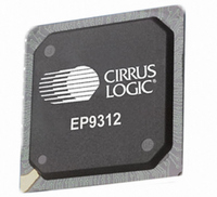
EP9312-IBZ Cirrus Logic Inc, EP9312-IBZ Datasheet - Page 662

EP9312-IBZ
Manufacturer Part Number
EP9312-IBZ
Description
IC ARM920T MCU 200MHZ 352-PBGA
Manufacturer
Cirrus Logic Inc
Series
EP9r
Specifications of EP9312-IBZ
Core Size
16/32-Bit
Package / Case
352-BGA
Core Processor
ARM9
Speed
200MHz
Connectivity
EBI/EMI, EIDE, Ethernet, I²C, IrDA, Keypad/Touchscreen, SPI, UART/USART, USB
Peripherals
AC'97, DMA, I²:S, LCD, LED, MaverickKey, POR, PWM, WDT
Number Of I /o
16
Program Memory Type
ROMless
Ram Size
32K x 8
Voltage - Supply (vcc/vdd)
1.65 V ~ 3.6 V
Data Converters
A/D 8x12b
Oscillator Type
External
Operating Temperature
-40°C ~ 85°C
Controller Family/series
(ARM9)
A/d Converter
12 Bits
No. Of I/o Pins
65
Clock Frequency
200MHz
Processor Series
EP93xx
Core
ARM920T
Data Bus Width
32 bit
3rd Party Development Tools
MDK-ARM, RL-ARM, ULINK2
Lead Free Status / RoHS Status
Lead free / RoHS Compliant
Eeprom Size
-
Program Memory Size
-
Lead Free Status / Rohs Status
Details
Other names
598-1260
Available stocks
Company
Part Number
Manufacturer
Quantity
Price
Company:
Part Number:
EP9312-IBZ
Manufacturer:
CIRRUS
Quantity:
30
Company:
Part Number:
EP9312-IBZ
Manufacturer:
HITTITE
Quantity:
1 200
- Current page: 662 of 824
- Download datasheet (13Mb)
21
21-6
I
EP93xx User’s Guide
21.3.1 Receiver FIFO’s
2
S Controller
The basic operation of the I
right words. This pair of words is written to a FIFO, which the ARM will read.
Each channel has a 16 deep by 32 bit wide FIFO where the ARM or DMA controller can read
up to 8 sets of left / right data pairs. In order to receive left and right stereo data into the FIFO
and read this data out from the FIFO, the following sequence of events must be performed by
the programmer:
• Programmable first data bit position. that is, I
• Programmable left or right data word justification.
• Programmable data shift direction, that is, MSB or LSB received first.
• Data overflow detection.
• Clock domain synchronization.
• DMA accesses.
1. Enable the I
2. Enable the receive channel.
PCLK to the I
the data line. After being enabled, the I
incoming left stereo word as indicated by the audio word clock. When the start of the left
word occurs, the I
dedicated left shift register. At the end of the left word and start of the right word as
indicated by the audio word clock, the contents of the left shift register are loaded into a
left data register. The I
into a dedicated right shift register. At the end of the right word and start of the next left
word, the contents of the right shift register are loaded into a right data register. One
complete left and right stereo sample has now been received.
written to the FIFO. The I
0, which consists of 2 x 32 bit registers (assuming that this is the first sample to be
received). The FIFO-empty bit in the I
now de-asserted. As more stereo sample pairs are received, they will be written to
locations 1, 2, 3 and so on.
any valid left / right stereo samples. These samples are obtained from the FIFO via the
APB by reading from the I2SRX0Lft and I2SRX0Rt registers. (See “Register
The I
The channel corresponding to the FIFO must be enabled in order for it to start sampling
At this point, the I
The programmer can determine from the Global Control Status register if the FIFO has
2
S global control register bit, I2SGlCtrl[0], must be written to in order to turn on the
2
S controller.
2
S controller. The I
2
2
S controller signals to the FIFO that there is valid data ready to be
S controller will sample the data line and load each bit into a
2
2
S receiver is that data is serially shifted in to form a pair of left /
S controller will continue to sample the data line loading each bit
Copyright 2007 Cirrus Logic
2
S controller will then write this stereo sample to FIFO location
2
S controller will not function correctly if this is not done.
2
S Global Control Status register (I2SGlSts) is
2
S controller will wait until the start of the next
2
S or non-I
2
S format.
DS785UM1
Related parts for EP9312-IBZ
Image
Part Number
Description
Manufacturer
Datasheet
Request
R

Part Number:
Description:
IC ARM9 SOC UNIVERSAL 352PBGA
Manufacturer:
Cirrus Logic Inc
Datasheet:

Part Number:
Description:
System-on-Chip Processor
Manufacturer:
Cirrus Logic Inc
Datasheet:

Part Number:
Description:
IC ARM920T MCU 200MHZ 352-PBGA
Manufacturer:
Cirrus Logic Inc
Datasheet:

Part Number:
Description:
Development Kit
Manufacturer:
Cirrus Logic Inc
Datasheet:

Part Number:
Description:
Development Kit
Manufacturer:
Cirrus Logic Inc
Datasheet:

Part Number:
Description:
High-efficiency PFC + Fluorescent Lamp Driver Reference Design
Manufacturer:
Cirrus Logic Inc
Datasheet:

Part Number:
Description:
Development Kit
Manufacturer:
Cirrus Logic Inc
Datasheet:

Part Number:
Description:
Development Kit
Manufacturer:
Cirrus Logic Inc
Datasheet:

Part Number:
Description:
Development Kit
Manufacturer:
Cirrus Logic Inc
Datasheet:

Part Number:
Description:
Development Kit
Manufacturer:
Cirrus Logic Inc
Datasheet:

Part Number:
Description:
Development Kit
Manufacturer:
Cirrus Logic Inc
Datasheet:

Part Number:
Description:
Development Kit
Manufacturer:
Cirrus Logic Inc
Datasheet:

Part Number:
Description:
Ref Bd For Speakerbar MSA & DSP Products
Manufacturer:
Cirrus Logic Inc


