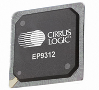
EP9312-IBZ Cirrus Logic Inc, EP9312-IBZ Datasheet - Page 41

EP9312-IBZ
Manufacturer Part Number
EP9312-IBZ
Description
IC ARM920T MCU 200MHZ 352-PBGA
Manufacturer
Cirrus Logic Inc
Series
EP9r
Specifications of EP9312-IBZ
Core Size
16/32-Bit
Package / Case
352-BGA
Core Processor
ARM9
Speed
200MHz
Connectivity
EBI/EMI, EIDE, Ethernet, I²C, IrDA, Keypad/Touchscreen, SPI, UART/USART, USB
Peripherals
AC'97, DMA, I²:S, LCD, LED, MaverickKey, POR, PWM, WDT
Number Of I /o
16
Program Memory Type
ROMless
Ram Size
32K x 8
Voltage - Supply (vcc/vdd)
1.65 V ~ 3.6 V
Data Converters
A/D 8x12b
Oscillator Type
External
Operating Temperature
-40°C ~ 85°C
Controller Family/series
(ARM9)
A/d Converter
12 Bits
No. Of I/o Pins
65
Clock Frequency
200MHz
Processor Series
EP93xx
Core
ARM920T
Data Bus Width
32 bit
3rd Party Development Tools
MDK-ARM, RL-ARM, ULINK2
Lead Free Status / RoHS Status
Lead free / RoHS Compliant
Eeprom Size
-
Program Memory Size
-
Lead Free Status / Rohs Status
Details
Other names
598-1260
Available stocks
Company
Part Number
Manufacturer
Quantity
Price
Company:
Part Number:
EP9312-IBZ
Manufacturer:
CIRRUS
Quantity:
30
Company:
Part Number:
EP9312-IBZ
Manufacturer:
HITTITE
Quantity:
1 200
- Current page: 41 of 824
- Download datasheet (13Mb)
DS785UM1
2.2.3.1 ARM9TDMI Core
A 16 kbyte instruction and a 16 kbyte data cache are included to increase performance for
cache-enabled memory regions. The 64-way associative cache also has lock-down
capability. A 16-word Write Buffer allows cached instructions to be fetched and decoded while
the Write Buffer sends data to external memory.
The ARM920T Core supports a number of co-processors, including the MaverickCrunch co-
processor by means of a specific pipeline architecture interface.
ARM9TDMI core is responsible for executing both 32-bit ARM and 16-bit Thumb instructions.
Each provides a unique advantage to a system design. Internally, the instructions enter a 5-
stage pipeline. These stages are:
All instructions are fully interlocked. This mechanism will delay the execution stage of a
instruction if data in that instruction comes from a previous instruction that is not available yet.
This simply insures that software will function identically across different implementations.
For memory access instructions, the base register used for the access will be restored by the
ARM Core in the event of an Abort exception. The base register will be restored to the value
contained in it immediately before execution of the instruction.
The ARM9TDMI core memory interface includes a separate instruction and data interface to
allow concurrent access of instructions and data to reduce the number of CPI (cycles per
instruction). Both interfaces use pipeline addressing. The core can operate in big and little
endian mode. Endianess affects both the address and the data interfaces.
The memory interface executes four types of memory transfers: sequential, non-sequential,
internal, and co-processor. It will also support uni- and bi-directional transfer modes.
The core provides a debug interface called JTAG (Joint Testing Action Group). This interface
provides debug capability with five external control signals:
There are six scan chains (0 through 5) in the ARM9TDMI controlled by the JTAG Test
Access Port (TAP) controller. Details on the individual scan chain function and bit order can
be found in the ARM920T Technical Reference Manual.
• Instruction Fetch
• Instruction Decode
• Execute
• Data Memory Access
• Register Write
• TDO - Test Data Out
• TDI - Test Data In
• TMS - Test Mode Select
• TCK - Test Clock
• nTRST - Test Reset
Copyright 2007 Cirrus Logic
ARM920T Core and Advanced High-Speed Bus (AHB)
EP93xx User’s Guide
2-3
2
Related parts for EP9312-IBZ
Image
Part Number
Description
Manufacturer
Datasheet
Request
R

Part Number:
Description:
IC ARM9 SOC UNIVERSAL 352PBGA
Manufacturer:
Cirrus Logic Inc
Datasheet:

Part Number:
Description:
System-on-Chip Processor
Manufacturer:
Cirrus Logic Inc
Datasheet:

Part Number:
Description:
IC ARM920T MCU 200MHZ 352-PBGA
Manufacturer:
Cirrus Logic Inc
Datasheet:

Part Number:
Description:
Development Kit
Manufacturer:
Cirrus Logic Inc
Datasheet:

Part Number:
Description:
Development Kit
Manufacturer:
Cirrus Logic Inc
Datasheet:

Part Number:
Description:
High-efficiency PFC + Fluorescent Lamp Driver Reference Design
Manufacturer:
Cirrus Logic Inc
Datasheet:

Part Number:
Description:
Development Kit
Manufacturer:
Cirrus Logic Inc
Datasheet:

Part Number:
Description:
Development Kit
Manufacturer:
Cirrus Logic Inc
Datasheet:

Part Number:
Description:
Development Kit
Manufacturer:
Cirrus Logic Inc
Datasheet:

Part Number:
Description:
Development Kit
Manufacturer:
Cirrus Logic Inc
Datasheet:

Part Number:
Description:
Development Kit
Manufacturer:
Cirrus Logic Inc
Datasheet:

Part Number:
Description:
Development Kit
Manufacturer:
Cirrus Logic Inc
Datasheet:

Part Number:
Description:
Ref Bd For Speakerbar MSA & DSP Products
Manufacturer:
Cirrus Logic Inc


