SAK-C505CA-4EM CA Infineon Technologies, SAK-C505CA-4EM CA Datasheet - Page 56
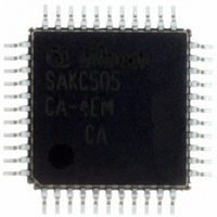
SAK-C505CA-4EM CA
Manufacturer Part Number
SAK-C505CA-4EM CA
Description
IC MCU 8BIT 32KB OTP MQFP-44-2
Manufacturer
Infineon Technologies
Series
C5xx/C8xxr
Datasheet
1.SAK-C505CA-4EM_CA.pdf
(88 pages)
Specifications of SAK-C505CA-4EM CA
Core Processor
C500
Core Size
8-Bit
Speed
20MHz
Connectivity
CAN, EBI/EMI, UART/USART
Peripherals
POR, PWM, WDT
Number Of I /o
34
Program Memory Size
32KB (32K x 8)
Program Memory Type
OTP
Ram Size
1.25K x 8
Voltage - Supply (vcc/vdd)
4.25 V ~ 5.5 V
Data Converters
A/D 8x10b
Oscillator Type
External
Operating Temperature
-40°C ~ 125°C
Package / Case
44-BQFP
Data Bus Width
8 bit
Data Ram Size
1.25 KB
Interface Type
CAN, USART
Maximum Clock Frequency
20 MHz
Number Of Programmable I/os
34
Number Of Timers
3
Maximum Operating Temperature
+ 125 C
Mounting Style
SMD/SMT
Minimum Operating Temperature
- 40 C
On-chip Adc
10 bit, 8 Channel
Packages
PG-MQFP-44
Max Clock Frequency
20.0 MHz
Sram (incl. Cache)
1.25 KByte
Can Nodes
1
A / D Input Lines (incl. Fadc)
8
Program Memory
32.0 KByte
Lead Free Status / RoHS Status
Lead free / RoHS Compliant
Eeprom Size
-
Lead Free Status / Rohs Status
Details
Other names
K505CA4EMCANP
K505CA4EMCAXT
SAK-C505CA-4EMCA
SAK-C505CA-4EMCAINTR
SAK-C505CA-4EMCATR
SAK-C505CA-4EMCATR
SAKC505CA4EMCAXT
SP000106397
K505CA4EMCAXT
SAK-C505CA-4EMCA
SAK-C505CA-4EMCAINTR
SAK-C505CA-4EMCATR
SAK-C505CA-4EMCATR
SAKC505CA4EMCAXT
SP000106397


The following
are required for OTP memory programming.
Table 11
Pin Definitions and Functions in Programming Mode
Symbol
RESET
PMSEL0
PMSEL1
PSEL
PRD
PALE
XTAL2
XTAL1
V
V
*) I = Input
Data Sheet
SS
DD
O = Output
Pin Number
4
5
7
8
9
10
14
15
16
17
Table 11
contains the functional description of all C505A-4E/C505CA-4E pins which
I/O
*)
I
I
I
I
I
I
O
I
–
–
Function
Reset
This input must be at static “1“ (active) level during the whole
programming mode.
Programming mode selection pins
These pins are used to select the different access modes in
programming mode. PMSEL1,0 must satisfy a setup time to the
rising edge of PALE. When the logic level of PMSEL1,0 is
changed, PALE must be at low level.
Basic programming mode select
This input is used for the basic programming mode selection
and must be switched according
Programming mode read strobe
This input is used for read access control for OTP memory read,
Version Register read, and lock bit read operations.
Programming address latch enable
PALE is used to latch the high address lines. The high address
lines must satisfy a setup and hold time to/from the falling edge
of PALE. PALE must be at low level when the logic level of
PMSEL1,0 is changed.
XTAL2
Output of the inverting oscillator amplifier.
XTAL1
Input to the oscillator amplifier.
Circuit ground potential
must be applied in programming mode.
Power supply terminal
must be applied in programming mode.
PMSEL1
0
0
1
1
52
PMSEL0
0
1
0
1
C505/C505C/C505A/C505CA
Access Mode
Reserved
Read version bytes
Program/read lock bits
Program/read OTP memory byte
Figure
28.
12.00
Related parts for SAK-C505CA-4EM CA
Image
Part Number
Description
Manufacturer
Datasheet
Request
R

Part Number:
Description:
Manufacturer:
Infineon Technologies AG
Datasheet:

Part Number:
Description:
Microcontrollers (MCU) 8-Bit Single Chip Microcontroller
Manufacturer:
Infineon Technologies
Datasheet:

Part Number:
Description:
Microcontrollers (MCU) 8-Bit Single Chip Microcontroller
Manufacturer:
Infineon Technologies

Part Number:
Description:
IC, 8BIT MCU, 32K OTP, SMD
Manufacturer:
Infineon Technologies
Datasheet:
Part Number:
Description:
Manufacturer:
Infineon Technologies AG
Datasheet:
Part Number:
Description:
Manufacturer:
Infineon Technologies AG
Datasheet:
Part Number:
Description:
Manufacturer:
Infineon Technologies AG
Datasheet:
Part Number:
Description:
Manufacturer:
Infineon Technologies AG
Datasheet:
Part Number:
Description:
Manufacturer:
Infineon Technologies AG
Datasheet:
Part Number:
Description:
Manufacturer:
Infineon Technologies AG
Datasheet:
Part Number:
Description:
Manufacturer:
Infineon Technologies AG
Datasheet:
Part Number:
Description:
16-bit microcontroller with 2x2 KByte RAM
Manufacturer:
Infineon Technologies AG
Datasheet:
Part Number:
Description:
NPN silicon RF transistor
Manufacturer:
Infineon Technologies AG
Datasheet:
Part Number:
Description:
NPN silicon RF transistor
Manufacturer:
Infineon Technologies AG
Datasheet: