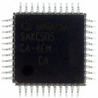
SAK-C505CA-4EM CA Infineon Technologies, SAK-C505CA-4EM CA Datasheet - Page 16
SAK-C505CA-4EM CA
Manufacturer Part Number
SAK-C505CA-4EM CA
Description
IC MCU 8BIT 32KB OTP MQFP-44-2
Manufacturer
Infineon Technologies
Series
C5xx/C8xxr
Datasheet
1.SAK-C505CA-4EM_CA.pdf
(88 pages)
Specifications of SAK-C505CA-4EM CA
Core Processor
C500
Core Size
8-Bit
Speed
20MHz
Connectivity
CAN, EBI/EMI, UART/USART
Peripherals
POR, PWM, WDT
Number Of I /o
34
Program Memory Size
32KB (32K x 8)
Program Memory Type
OTP
Ram Size
1.25K x 8
Voltage - Supply (vcc/vdd)
4.25 V ~ 5.5 V
Data Converters
A/D 8x10b
Oscillator Type
External
Operating Temperature
-40°C ~ 125°C
Package / Case
44-BQFP
Data Bus Width
8 bit
Data Ram Size
1.25 KB
Interface Type
CAN, USART
Maximum Clock Frequency
20 MHz
Number Of Programmable I/os
34
Number Of Timers
3
Maximum Operating Temperature
+ 125 C
Mounting Style
SMD/SMT
Minimum Operating Temperature
- 40 C
On-chip Adc
10 bit, 8 Channel
Packages
PG-MQFP-44
Max Clock Frequency
20.0 MHz
Sram (incl. Cache)
1.25 KByte
Can Nodes
1
A / D Input Lines (incl. Fadc)
8
Program Memory
32.0 KByte
Lead Free Status / RoHS Status
Lead free / RoHS Compliant
Eeprom Size
-
Lead Free Status / Rohs Status
Details
Other names
K505CA4EMCANP
K505CA4EMCAXT
SAK-C505CA-4EMCA
SAK-C505CA-4EMCAINTR
SAK-C505CA-4EMCATR
SAK-C505CA-4EMCATR
SAKC505CA4EMCAXT
SP000106397
K505CA4EMCAXT
SAK-C505CA-4EMCA
SAK-C505CA-4EMCAINTR
SAK-C505CA-4EMCATR
SAK-C505CA-4EMCATR
SAKC505CA4EMCAXT
SP000106397


CPU
The C505 is efficient both as a controller and as an arithmetic processor. It has extensive facilities
for binary and BCD arithmetic and excels in its bit-handling capabilities. Efficient use of program
memory results from an instruction set consisting of 44 % one-byte, 41 % two-byte, and 15% three-
byte instructions. With a 16 MHz crystal, 58% of the instructions are executed in 375 ns (20MHz:
300 ns).
Special Function Register PSW (Address D0 H )
Bit
CY
AC
F0
RS1
RS0
OV
F1
P
Data Sheet
D0 H
Bit No. MSB
D7 H
CY
Function
Carry Flag
Used by arithmetic instruction.
Auxiliary Carry Flag
Used by instructions which execute BCD operations.
General Purpose Flag
Register Bank Select Control Bits
These bits are used to select one of the four register banks.
Overflow Flag
Used by arithmetic instruction.
General Purpose Flag
Parity Flag
Set/cleared by hardware after each instruction to indicate an odd/even
number of "one" bits in the accumulator, i.e. even parity.
RS1
0
0
1
1
D6 H
AC
D5 H
F0
RS0
0
1
0
1
RS1
D4 H
Function
Bank 0 selected, data address 00 H -07 H
Bank 1 selected, data address 08 H -0F H
Bank 2 selected, data address 10 H -17 H
Bank 3 selected, data address 18 H -1F H
12
RS0
D3 H
D2 H
OV
C505/C505C/C505A/C505CA
D1 H
F1
LSB
D0 H
P
Reset Value : 00 H
PSW
12.00
Related parts for SAK-C505CA-4EM CA
Image
Part Number
Description
Manufacturer
Datasheet
Request
R

Part Number:
Description:
Manufacturer:
Infineon Technologies AG
Datasheet:

Part Number:
Description:
Microcontrollers (MCU) 8-Bit Single Chip Microcontroller
Manufacturer:
Infineon Technologies
Datasheet:

Part Number:
Description:
Microcontrollers (MCU) 8-Bit Single Chip Microcontroller
Manufacturer:
Infineon Technologies

Part Number:
Description:
IC, 8BIT MCU, 32K OTP, SMD
Manufacturer:
Infineon Technologies
Datasheet:
Part Number:
Description:
Manufacturer:
Infineon Technologies AG
Datasheet:
Part Number:
Description:
Manufacturer:
Infineon Technologies AG
Datasheet:
Part Number:
Description:
Manufacturer:
Infineon Technologies AG
Datasheet:
Part Number:
Description:
Manufacturer:
Infineon Technologies AG
Datasheet:
Part Number:
Description:
Manufacturer:
Infineon Technologies AG
Datasheet:
Part Number:
Description:
Manufacturer:
Infineon Technologies AG
Datasheet:
Part Number:
Description:
Manufacturer:
Infineon Technologies AG
Datasheet:
Part Number:
Description:
16-bit microcontroller with 2x2 KByte RAM
Manufacturer:
Infineon Technologies AG
Datasheet:
Part Number:
Description:
NPN silicon RF transistor
Manufacturer:
Infineon Technologies AG
Datasheet:
Part Number:
Description:
NPN silicon RF transistor
Manufacturer:
Infineon Technologies AG
Datasheet: