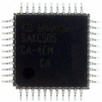
SAK-C505CA-4EM CA Infineon Technologies, SAK-C505CA-4EM CA Datasheet - Page 22
SAK-C505CA-4EM CA
Manufacturer Part Number
SAK-C505CA-4EM CA
Description
IC MCU 8BIT 32KB OTP MQFP-44-2
Manufacturer
Infineon Technologies
Series
C5xx/C8xxr
Datasheet
1.SAK-C505CA-4EM_CA.pdf
(88 pages)
Specifications of SAK-C505CA-4EM CA
Core Processor
C500
Core Size
8-Bit
Speed
20MHz
Connectivity
CAN, EBI/EMI, UART/USART
Peripherals
POR, PWM, WDT
Number Of I /o
34
Program Memory Size
32KB (32K x 8)
Program Memory Type
OTP
Ram Size
1.25K x 8
Voltage - Supply (vcc/vdd)
4.25 V ~ 5.5 V
Data Converters
A/D 8x10b
Oscillator Type
External
Operating Temperature
-40°C ~ 125°C
Package / Case
44-BQFP
Data Bus Width
8 bit
Data Ram Size
1.25 KB
Interface Type
CAN, USART
Maximum Clock Frequency
20 MHz
Number Of Programmable I/os
34
Number Of Timers
3
Maximum Operating Temperature
+ 125 C
Mounting Style
SMD/SMT
Minimum Operating Temperature
- 40 C
On-chip Adc
10 bit, 8 Channel
Packages
PG-MQFP-44
Max Clock Frequency
20.0 MHz
Sram (incl. Cache)
1.25 KByte
Can Nodes
1
A / D Input Lines (incl. Fadc)
8
Program Memory
32.0 KByte
Lead Free Status / RoHS Status
Lead free / RoHS Compliant
Eeprom Size
-
Lead Free Status / Rohs Status
Details
Other names
K505CA4EMCANP
K505CA4EMCAXT
SAK-C505CA-4EMCA
SAK-C505CA-4EMCAINTR
SAK-C505CA-4EMCATR
SAK-C505CA-4EMCATR
SAKC505CA4EMCAXT
SP000106397
K505CA4EMCAXT
SAK-C505CA-4EMCA
SAK-C505CA-4EMCAINTR
SAK-C505CA-4EMCATR
SAK-C505CA-4EMCATR
SAKC505CA4EMCAXT
SP000106397


Special Function Registers
The registers, except the program counter and the four general purpose register banks, reside in
the special function register area. The special function register area consists of two portions : the
standard special function register area and the mapped special function register area. Five special
function register of the C505 (PCON1,P1ANA, VR0, VR1, VR2) are located in the mapped special
function register area. For accessing the mapped special function register area, bit RMAP in special
function register SYSCON must be set. All other special function registers are located in the
standard special function register area which is accessed when RMAP is cleared (“0“).
The registers and data locations of the CAN controller (CAN-SFRs) are located in the external data
memory area at addresses F700 H to F7FF H ..
Special Function Register SYSCON (Address B1 H )
(C505CA only)
Bit
RMAP
CSWO
As long as bit RMAP is set, mapped special function register area can be accessed. This bit is not
cleared by hardware automatically. Thus, when non-mapped/mapped registers are to be accessed,
the bit RMAP must be cleared/set respectively by software.
All SFRs with addresses where address bits 0-2 are 0 (e.g. 80 H , 88 H , 90 H , 98 H , ..., F8 H , FF H ) are
bitaddressable.
The 52 special function registers (SFRs) in the standard and mapped SFR area include pointers
and registers that provide an interface between the CPU and the other on-chip peripherals. The
SFRs of the C505 are listed in
refer to the functional blocks of the C505. The CAN-SFRs (applicable for the C505C and C505CA
only) are also included in
their addresses.
Data Sheet
B1 H
Bit No. MSB
Function
Special function register map bit
RMAP = 0 : The access to the non-mapped (standard) special function register
RMAP = 1 : The access to the mapped special function register area is enabled.
CAN Controller switch-off bit
CSWO = 0 : CAN Controller is enabled (default after reset).
CSWO = 1 : CAN Controller is switched off.
Table 5
7
–
The functions of the shaded bits are not described here.
1) This bit is only available in the C505CA.
list the CAN-SFRs in numeric order of their addresses.
Table
6
–
area is enabled.
Table 3
EALE RMAP CMOD
3.
5
Table 4
and
4
Table
illustrates the contents of the SFRs in numeric order of
18
4. In
3
Table 3
CSWO XMAP1
1)
2
C505/C505C/C505A/C505CA
they are organized in groups which
1
Reset Value : XX100X01 B
Reset Value : XX100001 B
XMAP0
LSB
0
SYSCON
12.00
Related parts for SAK-C505CA-4EM CA
Image
Part Number
Description
Manufacturer
Datasheet
Request
R

Part Number:
Description:
Manufacturer:
Infineon Technologies AG
Datasheet:

Part Number:
Description:
Microcontrollers (MCU) 8-Bit Single Chip Microcontroller
Manufacturer:
Infineon Technologies
Datasheet:

Part Number:
Description:
Microcontrollers (MCU) 8-Bit Single Chip Microcontroller
Manufacturer:
Infineon Technologies

Part Number:
Description:
IC, 8BIT MCU, 32K OTP, SMD
Manufacturer:
Infineon Technologies
Datasheet:
Part Number:
Description:
Manufacturer:
Infineon Technologies AG
Datasheet:
Part Number:
Description:
Manufacturer:
Infineon Technologies AG
Datasheet:
Part Number:
Description:
Manufacturer:
Infineon Technologies AG
Datasheet:
Part Number:
Description:
Manufacturer:
Infineon Technologies AG
Datasheet:
Part Number:
Description:
Manufacturer:
Infineon Technologies AG
Datasheet:
Part Number:
Description:
Manufacturer:
Infineon Technologies AG
Datasheet:
Part Number:
Description:
Manufacturer:
Infineon Technologies AG
Datasheet:
Part Number:
Description:
16-bit microcontroller with 2x2 KByte RAM
Manufacturer:
Infineon Technologies AG
Datasheet:
Part Number:
Description:
NPN silicon RF transistor
Manufacturer:
Infineon Technologies AG
Datasheet:
Part Number:
Description:
NPN silicon RF transistor
Manufacturer:
Infineon Technologies AG
Datasheet: