SAK-C505CA-4EM CA Infineon Technologies, SAK-C505CA-4EM CA Datasheet - Page 35
SAK-C505CA-4EM CA
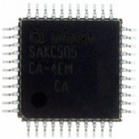
Manufacturer Part Number
SAK-C505CA-4EM CA
Description
IC MCU 8BIT 32KB OTP MQFP-44-2
Manufacturer
Infineon Technologies
Series
C5xx/C8xxr
Datasheet
1.SAK-C505CA-4EM_CA.pdf
(88 pages)
Specifications of SAK-C505CA-4EM CA
Core Processor
C500
Core Size
8-Bit
Speed
20MHz
Connectivity
CAN, EBI/EMI, UART/USART
Peripherals
POR, PWM, WDT
Number Of I /o
34
Program Memory Size
32KB (32K x 8)
Program Memory Type
OTP
Ram Size
1.25K x 8
Voltage - Supply (vcc/vdd)
4.25 V ~ 5.5 V
Data Converters
A/D 8x10b
Oscillator Type
External
Operating Temperature
-40°C ~ 125°C
Package / Case
44-BQFP
Data Bus Width
8 bit
Data Ram Size
1.25 KB
Interface Type
CAN, USART
Maximum Clock Frequency
20 MHz
Number Of Programmable I/os
34
Number Of Timers
3
Maximum Operating Temperature
+ 125 C
Mounting Style
SMD/SMT
Minimum Operating Temperature
- 40 C
On-chip Adc
10 bit, 8 Channel
Packages
PG-MQFP-44
Max Clock Frequency
20.0 MHz
Sram (incl. Cache)
1.25 KByte
Can Nodes
1
A / D Input Lines (incl. Fadc)
8
Program Memory
32.0 KByte
Lead Free Status / RoHS Status
Lead free / RoHS Compliant
Eeprom Size
-
Lead Free Status / Rohs Status
Details
Other names
K505CA4EMCANP
K505CA4EMCAXT
SAK-C505CA-4EMCA
SAK-C505CA-4EMCAINTR
SAK-C505CA-4EMCATR
SAK-C505CA-4EMCATR
SAKC505CA4EMCAXT
SP000106397
K505CA4EMCAXT
SAK-C505CA-4EMCA
SAK-C505CA-4EMCAINTR
SAK-C505CA-4EMCATR
SAK-C505CA-4EMCATR
SAKC505CA4EMCAXT
SP000106397


Timer 2 Compare Modes
The compare function of a timer/register combination operates as follows : the 16-bit value stored
in a compare or compare/capture register is compared with the contents of the timer register; if the
count value in the timer register matches the stored value, an appropriate output signal is generated
at a corresponding port pin and an interrupt can be generated.
Compare Mode 0
In compare mode 0, upon matching the timer and compare register contents, the output signal
changes from low to high. lt goes back to a low level on timer overflow. As long as compare mode
0 is enabled, the appropriate output pin is controlled by the timer circuit only and writing to the port
will have no effect.
mode 0. The port latch is directly controlled by the timer overflow and compare match signals. The
input line from the internal bus and the write-to-latch line of the port latch are disconnected when
compare mode 0 is enabled.
Figure 12
Port Latch in Compare Mode 0
Data Sheet
Compare Register
Timer Register
Compare Reg.
Timer Circuit
Comparator
Circuit
16 Bit
16
Bit
Figure 12
Compare
Match
Overflow
Timer
shows a functional diagram of a port circuit when used in compare
Port Circuit
Internal
Bus
Write to
Latch
31
C505/C505C/C505A/C505CA
S
D
CLK
R
Latch
Port
Read Pin
Read Latch
Q
Q
V
DD
MCS02661
Port
Pin
12.00
Related parts for SAK-C505CA-4EM CA
Image
Part Number
Description
Manufacturer
Datasheet
Request
R

Part Number:
Description:
Manufacturer:
Infineon Technologies AG
Datasheet:

Part Number:
Description:
Microcontrollers (MCU) 8-Bit Single Chip Microcontroller
Manufacturer:
Infineon Technologies
Datasheet:

Part Number:
Description:
Microcontrollers (MCU) 8-Bit Single Chip Microcontroller
Manufacturer:
Infineon Technologies

Part Number:
Description:
IC, 8BIT MCU, 32K OTP, SMD
Manufacturer:
Infineon Technologies
Datasheet:
Part Number:
Description:
Manufacturer:
Infineon Technologies AG
Datasheet:
Part Number:
Description:
Manufacturer:
Infineon Technologies AG
Datasheet:
Part Number:
Description:
Manufacturer:
Infineon Technologies AG
Datasheet:
Part Number:
Description:
Manufacturer:
Infineon Technologies AG
Datasheet:
Part Number:
Description:
Manufacturer:
Infineon Technologies AG
Datasheet:
Part Number:
Description:
Manufacturer:
Infineon Technologies AG
Datasheet:
Part Number:
Description:
Manufacturer:
Infineon Technologies AG
Datasheet:
Part Number:
Description:
16-bit microcontroller with 2x2 KByte RAM
Manufacturer:
Infineon Technologies AG
Datasheet:
Part Number:
Description:
NPN silicon RF transistor
Manufacturer:
Infineon Technologies AG
Datasheet:
Part Number:
Description:
NPN silicon RF transistor
Manufacturer:
Infineon Technologies AG
Datasheet: