SAK-C505CA-4EM CA Infineon Technologies, SAK-C505CA-4EM CA Datasheet - Page 39
SAK-C505CA-4EM CA
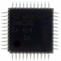
Manufacturer Part Number
SAK-C505CA-4EM CA
Description
IC MCU 8BIT 32KB OTP MQFP-44-2
Manufacturer
Infineon Technologies
Series
C5xx/C8xxr
Datasheet
1.SAK-C505CA-4EM_CA.pdf
(88 pages)
Specifications of SAK-C505CA-4EM CA
Core Processor
C500
Core Size
8-Bit
Speed
20MHz
Connectivity
CAN, EBI/EMI, UART/USART
Peripherals
POR, PWM, WDT
Number Of I /o
34
Program Memory Size
32KB (32K x 8)
Program Memory Type
OTP
Ram Size
1.25K x 8
Voltage - Supply (vcc/vdd)
4.25 V ~ 5.5 V
Data Converters
A/D 8x10b
Oscillator Type
External
Operating Temperature
-40°C ~ 125°C
Package / Case
44-BQFP
Data Bus Width
8 bit
Data Ram Size
1.25 KB
Interface Type
CAN, USART
Maximum Clock Frequency
20 MHz
Number Of Programmable I/os
34
Number Of Timers
3
Maximum Operating Temperature
+ 125 C
Mounting Style
SMD/SMT
Minimum Operating Temperature
- 40 C
On-chip Adc
10 bit, 8 Channel
Packages
PG-MQFP-44
Max Clock Frequency
20.0 MHz
Sram (incl. Cache)
1.25 KByte
Can Nodes
1
A / D Input Lines (incl. Fadc)
8
Program Memory
32.0 KByte
Lead Free Status / RoHS Status
Lead free / RoHS Compliant
Eeprom Size
-
Lead Free Status / Rohs Status
Details
Other names
K505CA4EMCANP
K505CA4EMCAXT
SAK-C505CA-4EMCA
SAK-C505CA-4EMCAINTR
SAK-C505CA-4EMCATR
SAK-C505CA-4EMCATR
SAKC505CA4EMCAXT
SP000106397
K505CA4EMCAXT
SAK-C505CA-4EMCA
SAK-C505CA-4EMCAINTR
SAK-C505CA-4EMCATR
SAK-C505CA-4EMCATR
SAKC505CA4EMCAXT
SP000106397


C505/C505C/C505A/C505CA
CAN Controller (C505C and C505CA only)
The on-chip CAN controller, compliant to version 2.0B, is the functional heart which provides all
resources that are required to run the standard CAN protocol (11-bit identifiers) as well as the
extended CAN protocol (29-bit identifiers). It provides a sophisticated object layer to relieve the
CPU of as much overhead as possible when controlling many different message objects (up to 15).
This includes bus arbitration, resending of garbled messages, error handling, interrupt generation,
etc. In order to implement the physical layer, external components have to be connected to the
C505C/C505CA.
The internal bus interface connects the on-chip CAN controller to the internal bus of the
microcontroller. The registers and data locations of the CAN interface are mapped to a specific 256
byte wide address range of the external data memory area (F700 H to F7FF H ) and can be accessed
using MOVX instructions.
Figure 15
shows a block diagram of the on-chip CAN controller.
The TX/RX Shift Register holds the destuffed bit stream from the bus line to allow the parallel
access to the whole data or remote frame for the acceptance match test and the parallel transfer of
the frame to and from the Intelligent Memory.
The Bit Stream Processor (BSP) is a sequencer controlling the sequential data stream between
the TX/RX Shift Register, the CRC Register, and the bus line. The BSP also controls the EML and
the parallel data stream between the TX/RX Shift Register and the Intelligent Memory such that the
processes of reception, arbitration, transmission, and error signalling are performed according to
the CAN protocol. Note that the automatic retransmission of messages which have been corrupted
by noise or other external error conditions on the bus line is handled by the BSP.
The Cyclic Redundancy Check Register (CRC) generates the Cyclic Redundancy Check code to
be transmitted after the data bytes and checks the CRC code of incoming messages. This is done
by dividing the data stream by the code generator polynomial.
The Error Management Logic (EML) is responsible for the fault confinement of the CAN device. Its
counters, the Receive Error Counter and the Transmit Error Counter, are incremented and
decremented by commands from the Bit Stream Processor. According to the values of the error
counters, the CAN controller is set into the states error active, error passive and busoff.
The Bit Timing Logic (BTL) monitors the busline input RXDC and handles the busline related bit
timing according to the CAN protocol. The BTL synchronizes on a recessive to dominant busline
transition at Start of Frame (hard synchronization) and on any further recessive to dominant busline
transition, if the CAN controller itself does not transmit a dominant bit (resynchronization). The BTL
also provides programmable time segments to compensate for the propagation delay time and for
phase shifts and to define the position of the Sample Point in the bit time. The programming of the
BTL depends on the baudrate and on external physical delay times.
The Intelligent Memory (CAM/RAM array) provides storage for up to 15 message objects of
maximum 8 data bytes length. Each of these objects has a unique identifier and its own set of
control and status bits. After the initial configuration, the Intelligent Memory can handle the
reception and transmission of data without further microcontroller actions.
Data Sheet
35
12.00
Related parts for SAK-C505CA-4EM CA
Image
Part Number
Description
Manufacturer
Datasheet
Request
R

Part Number:
Description:
Manufacturer:
Infineon Technologies AG
Datasheet:

Part Number:
Description:
Microcontrollers (MCU) 8-Bit Single Chip Microcontroller
Manufacturer:
Infineon Technologies
Datasheet:

Part Number:
Description:
Microcontrollers (MCU) 8-Bit Single Chip Microcontroller
Manufacturer:
Infineon Technologies

Part Number:
Description:
IC, 8BIT MCU, 32K OTP, SMD
Manufacturer:
Infineon Technologies
Datasheet:
Part Number:
Description:
Manufacturer:
Infineon Technologies AG
Datasheet:
Part Number:
Description:
Manufacturer:
Infineon Technologies AG
Datasheet:
Part Number:
Description:
Manufacturer:
Infineon Technologies AG
Datasheet:
Part Number:
Description:
Manufacturer:
Infineon Technologies AG
Datasheet:
Part Number:
Description:
Manufacturer:
Infineon Technologies AG
Datasheet:
Part Number:
Description:
Manufacturer:
Infineon Technologies AG
Datasheet:
Part Number:
Description:
Manufacturer:
Infineon Technologies AG
Datasheet:
Part Number:
Description:
16-bit microcontroller with 2x2 KByte RAM
Manufacturer:
Infineon Technologies AG
Datasheet:
Part Number:
Description:
NPN silicon RF transistor
Manufacturer:
Infineon Technologies AG
Datasheet:
Part Number:
Description:
NPN silicon RF transistor
Manufacturer:
Infineon Technologies AG
Datasheet: