MCF5407CAI220 Freescale Semiconductor, MCF5407CAI220 Datasheet - Page 68
MCF5407CAI220
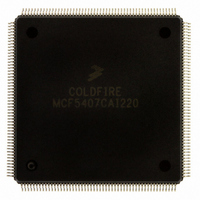
Manufacturer Part Number
MCF5407CAI220
Description
IC MPU 32B 220MHZ COLDF 208-FQFP
Manufacturer
Freescale Semiconductor
Series
MCF540xr
Specifications of MCF5407CAI220
Core Processor
Coldfire V4
Core Size
32-Bit
Speed
220MHz
Connectivity
EBI/EMI, I²C, UART/USART
Peripherals
DMA, WDT
Number Of I /o
16
Program Memory Type
ROMless
Ram Size
4K x 8
Voltage - Supply (vcc/vdd)
1.65 V ~ 3.6 V
Oscillator Type
External
Operating Temperature
-40°C ~ 85°C
Package / Case
208-FQFP
Processor Series
MCF540x
Core
ColdFire V4
Data Bus Width
32 bit
Program Memory Size
8 KB
Data Ram Size
4 KB
Maximum Clock Frequency
162 MHz
Number Of Programmable I/os
16
Operating Supply Voltage
1.8 V to 3.3 V
Mounting Style
SMD/SMT
3rd Party Development Tools
JLINK-CF-BDM26, EWCF
Cpu Speed
220MHz
Embedded Interface Type
I2C, UART
Digital Ic Case Style
FQFP
No. Of Pins
208
Supply Voltage Range
3.3V
Rohs Compliant
Yes
For Use With
M5407C3 - KIT EVAL FOR MCF5407 W/ETHERNET
Lead Free Status / RoHS Status
Lead free / RoHS Compliant
Eeprom Size
-
Program Memory Size
-
Data Converters
-
Lead Free Status / Rohs Status
Lead free / RoHS Compliant
Available stocks
Company
Part Number
Manufacturer
Quantity
Price
Company:

Part Number:
MCF5407CAI220
Manufacturer:
Freescale
Quantity:
789
Company:
Part Number:
MCF5407CAI220
Manufacturer:
Freescale Semiconductor
Quantity:
10 000


Features and Enhancements
2.1.1 Clock-Multiplied Microprocessor Core
The MCF5407 incorporates a clock-multiplying phase-locked loop (PLL). Increasing the
internal speed of the core also allows higher performance while providing the system
designer with an easy-to-use lower speed system interface.
The frequency of the processor complex is an integer multiple of the external bus speed.
Chapter 20, “Electrical Specifications,” lists the supported clock ratios.
The processor, instruction and data caches, integrated SRAMs, and misalignment module
operate at the higher speed clock (PCLK); other system integrated modules operate at the
speed of the input clock (CLKIN). When combined with the enhanced pipeline structure of
the Version 4 ColdFire core, the processor and its local memories provide a high level of
performance for today’s demanding embedded applications.
PCLK can be disabled to minimize dissipation when a low-power mode is entered. This is
described in Section 7.2.3, “Reduced-Power Mode.”
2.1.2 Enhanced Pipelines
The IFP prefetches instructions. The OEP decodes instructions, fetches required operands,
then executes the specified function. The two independent, decoupled pipeline structures
maximize performance while minimizing core size. Pipeline stages are shown in Figure 2-1
and are summarized as follows:
2-2
• Vector base register to relocate exception-vector table
• Optimized for high-level language constructs
• Four-stage IFP (plus optional instruction buffer stage)
• Five-stage OEP with two optional processor bus write cycles.
— Instruction address generation (IAG) calculates the next prefetch address.
— Instruction fetch cycle 1 (IC1) initiates prefetch on the processor’s local
— Instruction fetch cycle 2 (IC2) completes prefetch on the processor’s instruction
— Instruction early decode (IED) generates time-critical decode signals needed for
— Instruction buffer (IB) optional stage uses FIFO queue to minimize effects of
— Decode stage (DS/secDS) decodes and selects for two sequential instructions.
— Operand address generation (OAG) generates the address for the data operand.
— Operand fetch cycle 1 and 2 (OC1 and OC2) fetch data operands.
— Execute (EX) performs prescribed operations on previously fetched data
instruction bus.
local bus.
the OEP.
fetch latency.
operands.
MCF5407 User’s Manual
Related parts for MCF5407CAI220
Image
Part Number
Description
Manufacturer
Datasheet
Request
R

Part Number:
Description:
Mcf5407 Coldfire Integrated Microprocessor User
Manufacturer:
Freescale Semiconductor, Inc
Datasheet:
Part Number:
Description:
Manufacturer:
Freescale Semiconductor, Inc
Datasheet:
Part Number:
Description:
Manufacturer:
Freescale Semiconductor, Inc
Datasheet:
Part Number:
Description:
Manufacturer:
Freescale Semiconductor, Inc
Datasheet:
Part Number:
Description:
Manufacturer:
Freescale Semiconductor, Inc
Datasheet:
Part Number:
Description:
Manufacturer:
Freescale Semiconductor, Inc
Datasheet:
Part Number:
Description:
Manufacturer:
Freescale Semiconductor, Inc
Datasheet:
Part Number:
Description:
Manufacturer:
Freescale Semiconductor, Inc
Datasheet:
Part Number:
Description:
Manufacturer:
Freescale Semiconductor, Inc
Datasheet:
Part Number:
Description:
Manufacturer:
Freescale Semiconductor, Inc
Datasheet:
Part Number:
Description:
Manufacturer:
Freescale Semiconductor, Inc
Datasheet:
Part Number:
Description:
Manufacturer:
Freescale Semiconductor, Inc
Datasheet:
Part Number:
Description:
Manufacturer:
Freescale Semiconductor, Inc
Datasheet:
Part Number:
Description:
Manufacturer:
Freescale Semiconductor, Inc
Datasheet:
Part Number:
Description:
Manufacturer:
Freescale Semiconductor, Inc
Datasheet: