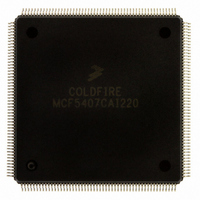
MCF5407CAI220 Freescale Semiconductor, MCF5407CAI220 Datasheet - Page 388

MCF5407CAI220
Manufacturer Part Number
MCF5407CAI220
Description
IC MPU 32B 220MHZ COLDF 208-FQFP
Manufacturer
Freescale Semiconductor
Series
MCF540xr
Specifications of MCF5407CAI220
Core Processor
Coldfire V4
Core Size
32-Bit
Speed
220MHz
Connectivity
EBI/EMI, I²C, UART/USART
Peripherals
DMA, WDT
Number Of I /o
16
Program Memory Type
ROMless
Ram Size
4K x 8
Voltage - Supply (vcc/vdd)
1.65 V ~ 3.6 V
Oscillator Type
External
Operating Temperature
-40°C ~ 85°C
Package / Case
208-FQFP
Processor Series
MCF540x
Core
ColdFire V4
Data Bus Width
32 bit
Program Memory Size
8 KB
Data Ram Size
4 KB
Maximum Clock Frequency
162 MHz
Number Of Programmable I/os
16
Operating Supply Voltage
1.8 V to 3.3 V
Mounting Style
SMD/SMT
3rd Party Development Tools
JLINK-CF-BDM26, EWCF
Cpu Speed
220MHz
Embedded Interface Type
I2C, UART
Digital Ic Case Style
FQFP
No. Of Pins
208
Supply Voltage Range
3.3V
Rohs Compliant
Yes
For Use With
M5407C3 - KIT EVAL FOR MCF5407 W/ETHERNET
Lead Free Status / RoHS Status
Lead free / RoHS Compliant
Eeprom Size
-
Program Memory Size
-
Data Converters
-
Lead Free Status / Rohs Status
Lead free / RoHS Compliant
Available stocks
Company
Part Number
Manufacturer
Quantity
Price
Company:
Part Number:
MCF5407CAI220
Manufacturer:
Freescale
Quantity:
789
Company:
Part Number:
MCF5407CAI220
Manufacturer:
Freescale Semiconductor
Quantity:
10 000
- Current page: 388 of 546
- Download datasheet (7Mb)
Parallel Port Operation
15.1.2 Port A Data Direction Register (PADDR)
The PADDR determines the signal direction of each parallel port pin programmed as a
general-purpose I/O port in the PAR.
Table 15-2 describes PADDR fields.
15.1.3 Port A Data Register (PADAT)
The PADAT value for inputs corresponds to the logic level at the pin; for outputs, the value
corresponds to the logic level driven onto the pin. Note the following:
PP[15:8]/
A[31:24]
TIP/PP7
DREQ[1:0]/
PP[6:5]
TM[2:0]/
PP[4:2]/
DACK[1:0]
TT[1:0]/
PP[1:0]
15-2
15–0
Bits
• PADAT has no effect on pins not configured for general-purpose I/O.
Pin
Address
PADDR
Name
Reset
Field
R/W
MSB of the address bus/parallel port. Programmed through PAR[15–8]. If a PAR bit is 0, the associated
pin functions as a parallel port signal. If a bit is 1, the pin functions as an address bus signal. If all pins
are address signals, as much as 4 Gbytes of memory space are available.
Transfer-in-progress output/parallel port bit 7. Programmed through PAR[7]. Assertion indicates a bus
transfer is in progress; negation indicates an idle bus cycle if the bus is still granted to the processor.
Note that TIP is held asserted on back-to-back bus cycles.
DMA request inputs/two bits of the parallel port. Programmed through PAR[6–5]. These inputs are
asserted by a peripheral device to request a DMA transfer.
Transfer type outputs/parallel port bits 4–2. Programmed through PAR[4–2]. For DMA transfers, these
signals provide acknowledge information or can be programmed to function as DMA acknowledge
signals. For emulation transfers, TM[2:0] indicate user or data transfer types. For CPU space transfers,
TM[2:0] are low. For interrupt acknowledge transfers, TM[2:0] carry the interrupt level being
acknowledged.
Transfer type outputs/parallel port bits 1–0. Programmed through PAR[1–0].
When the MCF5407 is bus master, it outputs these signals. They indicate the current bus access type.
15
Data direction bits. Each data direction bit selects the direction of the signal as follows:
0 Signal is defined as an input.
1 Signal is defined as an output.
Figure 15-2. Port A Data Direction Register (PADDR)
Table 15-1. Parallel Port Pin Descriptions
Table 15-2. PADDR Field Description
MCF5407 User’s Manual
Address MBAR + 0x244
0000_0000_0000_0000
Description
PADDR
Description
R/W
0
Related parts for MCF5407CAI220
Image
Part Number
Description
Manufacturer
Datasheet
Request
R
Part Number:
Description:
Mcf5407 Coldfire Integrated Microprocessor User
Manufacturer:
Freescale Semiconductor, Inc
Datasheet:
Part Number:
Description:
Manufacturer:
Freescale Semiconductor, Inc
Datasheet:
Part Number:
Description:
Manufacturer:
Freescale Semiconductor, Inc
Datasheet:
Part Number:
Description:
Manufacturer:
Freescale Semiconductor, Inc
Datasheet:
Part Number:
Description:
Manufacturer:
Freescale Semiconductor, Inc
Datasheet:
Part Number:
Description:
Manufacturer:
Freescale Semiconductor, Inc
Datasheet:
Part Number:
Description:
Manufacturer:
Freescale Semiconductor, Inc
Datasheet:
Part Number:
Description:
Manufacturer:
Freescale Semiconductor, Inc
Datasheet:
Part Number:
Description:
Manufacturer:
Freescale Semiconductor, Inc
Datasheet:
Part Number:
Description:
Manufacturer:
Freescale Semiconductor, Inc
Datasheet:
Part Number:
Description:
Manufacturer:
Freescale Semiconductor, Inc
Datasheet:
Part Number:
Description:
Manufacturer:
Freescale Semiconductor, Inc
Datasheet:
Part Number:
Description:
Manufacturer:
Freescale Semiconductor, Inc
Datasheet:
Part Number:
Description:
Manufacturer:
Freescale Semiconductor, Inc
Datasheet:
Part Number:
Description:
Manufacturer:
Freescale Semiconductor, Inc
Datasheet:


