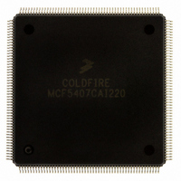
MCF5407CAI220 Freescale Semiconductor, MCF5407CAI220 Datasheet - Page 147

MCF5407CAI220
Manufacturer Part Number
MCF5407CAI220
Description
IC MPU 32B 220MHZ COLDF 208-FQFP
Manufacturer
Freescale Semiconductor
Series
MCF540xr
Specifications of MCF5407CAI220
Core Processor
Coldfire V4
Core Size
32-Bit
Speed
220MHz
Connectivity
EBI/EMI, I²C, UART/USART
Peripherals
DMA, WDT
Number Of I /o
16
Program Memory Type
ROMless
Ram Size
4K x 8
Voltage - Supply (vcc/vdd)
1.65 V ~ 3.6 V
Oscillator Type
External
Operating Temperature
-40°C ~ 85°C
Package / Case
208-FQFP
Processor Series
MCF540x
Core
ColdFire V4
Data Bus Width
32 bit
Program Memory Size
8 KB
Data Ram Size
4 KB
Maximum Clock Frequency
162 MHz
Number Of Programmable I/os
16
Operating Supply Voltage
1.8 V to 3.3 V
Mounting Style
SMD/SMT
3rd Party Development Tools
JLINK-CF-BDM26, EWCF
Cpu Speed
220MHz
Embedded Interface Type
I2C, UART
Digital Ic Case Style
FQFP
No. Of Pins
208
Supply Voltage Range
3.3V
Rohs Compliant
Yes
For Use With
M5407C3 - KIT EVAL FOR MCF5407 W/ETHERNET
Lead Free Status / RoHS Status
Lead free / RoHS Compliant
Eeprom Size
-
Program Memory Size
-
Data Converters
-
Lead Free Status / Rohs Status
Lead free / RoHS Compliant
Available stocks
Company
Part Number
Manufacturer
Quantity
Price
Company:
Part Number:
MCF5407CAI220
Manufacturer:
Freescale
Quantity:
789
Company:
Part Number:
MCF5407CAI220
Manufacturer:
Freescale Semiconductor
Quantity:
10 000
- Current page: 147 of 546
- Download datasheet (7Mb)
4.10.2 Access Control Registers (ACR0–ACR3)
The ACRs, Figure 4-9, assign control attributes, such as cache mode and write protection,
to specified memory regions. ACR0 and ACR1 control data attributes; ACR2 and ACR3
control instruction attributes. Registers are accessed with the MOVEC instruction with the
Rc encodings in Figure 4-9.
For overlapping data regions, ACR0 takes priority; ACR2 takes priority for overlapping
instruction regions. Data transfers to and from these registers are longword transfers. Bits
12–7, 4, 3, 1, and 0 are always read as zeros.
11
10
9
8
7–0
Bits
IHLCK
IDCM
—
ICINVA
—
Name
The SIM MBAR region should be mapped as cache-inhibited
through an ACR.
Instruction cache half-lock.
0 Normal operation. The cache allocates to the lowest invalid way; if all ways are valid, the cache
1 Half cache operation. The cache allocates to the lowest invalid way of ways 2 and 3; if both of
This implementation allows maximum use of the available cache memory and also provides the
flexibility of setting IHLCK before, during, or after the needed allocations occur.
Instruction default cache mode. For normal operations that do not hit in the RAMBARs or ACRs,
this field defines the effective cache mode.
0 Cacheable
1 Cache-inhibited
Reserved, should be cleared.
Instruction cache invalidate. Invalidation occurs when this bit is written as a 1. Note the caches
are not cleared on power-up or normal reset.
0 No invalidation is performed.
1 Initiate invalidation of instruction cache. The cache controller sequentially clears all V bits.
Reserved. These bits must be cleared; otherwise, performance may be affected.
allocates to the way pointed at by the round-robin counter and then increments this counter
modulo-4.
these ways are valid, the cache allocates to way 2 if the high-order bit of the round-robin
counter is zero; otherwise, it allocates way 3 and then increments the round-robin counter
modulo-2. This locks the content of ways 0 and 1. Ways 0 and 1 are still updated on write hits
and may be pushed or cleared by specific cache push/invalidate instructions.
Subsequent local memory bus accesses stall until invalidation completes, at which point,
ICINVA is cleared automatically without software intervention. For copyback mode, use
CPUSHL before setting ICINVA.
Table 4-4. CACR Field Descriptions (Continued)
Chapter 4. Local Memory
NOTE:
Description
Cache Registers
4-23
Related parts for MCF5407CAI220
Image
Part Number
Description
Manufacturer
Datasheet
Request
R
Part Number:
Description:
Mcf5407 Coldfire Integrated Microprocessor User
Manufacturer:
Freescale Semiconductor, Inc
Datasheet:
Part Number:
Description:
Manufacturer:
Freescale Semiconductor, Inc
Datasheet:
Part Number:
Description:
Manufacturer:
Freescale Semiconductor, Inc
Datasheet:
Part Number:
Description:
Manufacturer:
Freescale Semiconductor, Inc
Datasheet:
Part Number:
Description:
Manufacturer:
Freescale Semiconductor, Inc
Datasheet:
Part Number:
Description:
Manufacturer:
Freescale Semiconductor, Inc
Datasheet:
Part Number:
Description:
Manufacturer:
Freescale Semiconductor, Inc
Datasheet:
Part Number:
Description:
Manufacturer:
Freescale Semiconductor, Inc
Datasheet:
Part Number:
Description:
Manufacturer:
Freescale Semiconductor, Inc
Datasheet:
Part Number:
Description:
Manufacturer:
Freescale Semiconductor, Inc
Datasheet:
Part Number:
Description:
Manufacturer:
Freescale Semiconductor, Inc
Datasheet:
Part Number:
Description:
Manufacturer:
Freescale Semiconductor, Inc
Datasheet:
Part Number:
Description:
Manufacturer:
Freescale Semiconductor, Inc
Datasheet:
Part Number:
Description:
Manufacturer:
Freescale Semiconductor, Inc
Datasheet:
Part Number:
Description:
Manufacturer:
Freescale Semiconductor, Inc
Datasheet:


