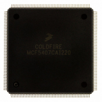
MCF5407CAI220 Freescale Semiconductor, MCF5407CAI220 Datasheet - Page 327

MCF5407CAI220
Manufacturer Part Number
MCF5407CAI220
Description
IC MPU 32B 220MHZ COLDF 208-FQFP
Manufacturer
Freescale Semiconductor
Series
MCF540xr
Specifications of MCF5407CAI220
Core Processor
Coldfire V4
Core Size
32-Bit
Speed
220MHz
Connectivity
EBI/EMI, I²C, UART/USART
Peripherals
DMA, WDT
Number Of I /o
16
Program Memory Type
ROMless
Ram Size
4K x 8
Voltage - Supply (vcc/vdd)
1.65 V ~ 3.6 V
Oscillator Type
External
Operating Temperature
-40°C ~ 85°C
Package / Case
208-FQFP
Processor Series
MCF540x
Core
ColdFire V4
Data Bus Width
32 bit
Program Memory Size
8 KB
Data Ram Size
4 KB
Maximum Clock Frequency
162 MHz
Number Of Programmable I/os
16
Operating Supply Voltage
1.8 V to 3.3 V
Mounting Style
SMD/SMT
3rd Party Development Tools
JLINK-CF-BDM26, EWCF
Cpu Speed
220MHz
Embedded Interface Type
I2C, UART
Digital Ic Case Style
FQFP
No. Of Pins
208
Supply Voltage Range
3.3V
Rohs Compliant
Yes
For Use With
M5407C3 - KIT EVAL FOR MCF5407 W/ETHERNET
Lead Free Status / RoHS Status
Lead free / RoHS Compliant
Eeprom Size
-
Program Memory Size
-
Data Converters
-
Lead Free Status / Rohs Status
Lead free / RoHS Compliant
Available stocks
Company
Part Number
Manufacturer
Quantity
Price
Company:
Part Number:
MCF5407CAI220
Manufacturer:
Freescale
Quantity:
789
Company:
Part Number:
MCF5407CAI220
Manufacturer:
Freescale Semiconductor
Quantity:
10 000
- Current page: 327 of 546
- Download datasheet (7Mb)
Although Figure 12-11 does not show TM0/DACK0 signaling a DMA acknowledgement,
this signal can provide an external request acknowledge response, as shown in subsequent
diagrams.
To initiate a request, DREQ need only be asserted long enough to be sampled on one rising
clock edge. However, note the following regarding the negation of DREQ:
Figure 12-12 shows a dual-address, peripheral-to-SDRAM DMA transfer. The DMA is not
parked on the bus, so the diagram shows how the CPU can generate multiple bus cycles
during DMA transfers. It also shows TM0/DACK0 timing. The TT signals indicate whether
the CPU (0) or DMA (1) has bus mastership. TM2 indicates dual-address mode.
If DCR[AT] is 1, TM/DACK is asserted during the final transfer. If DCR[AT] is 0,
TM/DACK asserts during all DMA accesses.
• In cycle-steal mode (DCR[CS] = 1), the read/write transaction is limited to a single
• In burst mode, (DCR[CS] = 0), multiple read/write transfers can occur on the bus as
TM0/DACK0
transfer. DREQ must be negated appropriately to avoid generating another request.
— For dual-address transfers, DREQ must be negated before TS is asserted for the
— For single-address transfers, DREQ must be negated before TS is asserted for the
programmed. DREQ need not be negated until DSR[DONE] is set, indicating the
block transfer is complete. Another transfer cannot be initiated until the DMA
registers are reprogrammed.
Figure 12-11. DREQ Timing Constraints, Dual-Address DMA Transfer
DREQ0
A[31:0]
CLKIN
write portion, as shown in Figure 12-11, clock cycle 7.
transfer, as shown in Figure 12-13, clock cycle 4.
R/W
TT1
TT0
CS
TS
TA
0
1
Chapter 12. DMA Controller Module
2
3
4
5
DMA Controller Module Functional Description
Read
6
7
8
9
Write
10
11
12-15
Related parts for MCF5407CAI220
Image
Part Number
Description
Manufacturer
Datasheet
Request
R
Part Number:
Description:
Mcf5407 Coldfire Integrated Microprocessor User
Manufacturer:
Freescale Semiconductor, Inc
Datasheet:
Part Number:
Description:
Manufacturer:
Freescale Semiconductor, Inc
Datasheet:
Part Number:
Description:
Manufacturer:
Freescale Semiconductor, Inc
Datasheet:
Part Number:
Description:
Manufacturer:
Freescale Semiconductor, Inc
Datasheet:
Part Number:
Description:
Manufacturer:
Freescale Semiconductor, Inc
Datasheet:
Part Number:
Description:
Manufacturer:
Freescale Semiconductor, Inc
Datasheet:
Part Number:
Description:
Manufacturer:
Freescale Semiconductor, Inc
Datasheet:
Part Number:
Description:
Manufacturer:
Freescale Semiconductor, Inc
Datasheet:
Part Number:
Description:
Manufacturer:
Freescale Semiconductor, Inc
Datasheet:
Part Number:
Description:
Manufacturer:
Freescale Semiconductor, Inc
Datasheet:
Part Number:
Description:
Manufacturer:
Freescale Semiconductor, Inc
Datasheet:
Part Number:
Description:
Manufacturer:
Freescale Semiconductor, Inc
Datasheet:
Part Number:
Description:
Manufacturer:
Freescale Semiconductor, Inc
Datasheet:
Part Number:
Description:
Manufacturer:
Freescale Semiconductor, Inc
Datasheet:
Part Number:
Description:
Manufacturer:
Freescale Semiconductor, Inc
Datasheet:


