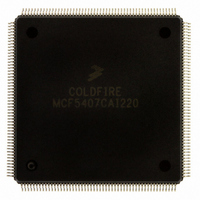
MCF5407CAI220 Freescale Semiconductor, MCF5407CAI220 Datasheet - Page 302

MCF5407CAI220
Manufacturer Part Number
MCF5407CAI220
Description
IC MPU 32B 220MHZ COLDF 208-FQFP
Manufacturer
Freescale Semiconductor
Series
MCF540xr
Specifications of MCF5407CAI220
Core Processor
Coldfire V4
Core Size
32-Bit
Speed
220MHz
Connectivity
EBI/EMI, I²C, UART/USART
Peripherals
DMA, WDT
Number Of I /o
16
Program Memory Type
ROMless
Ram Size
4K x 8
Voltage - Supply (vcc/vdd)
1.65 V ~ 3.6 V
Oscillator Type
External
Operating Temperature
-40°C ~ 85°C
Package / Case
208-FQFP
Processor Series
MCF540x
Core
ColdFire V4
Data Bus Width
32 bit
Program Memory Size
8 KB
Data Ram Size
4 KB
Maximum Clock Frequency
162 MHz
Number Of Programmable I/os
16
Operating Supply Voltage
1.8 V to 3.3 V
Mounting Style
SMD/SMT
3rd Party Development Tools
JLINK-CF-BDM26, EWCF
Cpu Speed
220MHz
Embedded Interface Type
I2C, UART
Digital Ic Case Style
FQFP
No. Of Pins
208
Supply Voltage Range
3.3V
Rohs Compliant
Yes
For Use With
M5407C3 - KIT EVAL FOR MCF5407 W/ETHERNET
Lead Free Status / RoHS Status
Lead free / RoHS Compliant
Eeprom Size
-
Program Memory Size
-
Data Converters
-
Lead Free Status / Rohs Status
Lead free / RoHS Compliant
Available stocks
Company
Part Number
Manufacturer
Quantity
Price
Company:
Part Number:
MCF5407CAI220
Manufacturer:
Freescale
Quantity:
789
Company:
Part Number:
MCF5407CAI220
Manufacturer:
Freescale Semiconductor
Quantity:
10 000
- Current page: 302 of 546
- Download datasheet (7Mb)
SDRAM Example
access can be a read or write. The important thing is that the address output of that access
needs the correct mode programming information on the correct address bits.
Figure 11-24 shows the
11.5 SDRAM Example
This example interfaces a 2M x 32-bit x 4 bank SDRAM component to a MCF5407
operating at 40 MHz. Table 11-32 lists design specifications for this example.
11.5.1 SDRAM Interface Configuration
To interface this component to the MCF5407 DRAM controller, use the connection table
that corresponds to a 32-bit port size with 8 columns (Table 11-26). Two pins select one of
four banks when the part is functional. Table 11-33 shows the proper hardware hook-up.
11-34
Speed grade (-8E)
10 rows, 8 columns
Two bank-select lines to access four internal banks
ACTV
Period between auto refresh and
ACTV
Precharge command to
Last data input to
Auto refresh period for 4096 rows (t
-to-read/write delay (t
command to precharge command (t
Figure 11-24. Mode Register Set (
Table 11-32. SDRAM Example Specifications
SRAS, SCAS
RAS[1] or [0]
MRS
PALL
DRAMW
D[31:0]
A[31:0]
CLKIN
command, which occurs in the first clock of the bus cycle.
command (t
Parameter
ACTV
RCD
command (t
)
MCF5407 User’s Manual
ACTV
RWL
REF
MRS
command (t
)
)
RAS
RP
)
)
RC
)
MRS
40 MHz (25-nS period)
20 nS (min.)
70 nS
48 nS (min.)
20 nS (min.)
1 bus clock (25 nS)
64 mS
) Command
Specification
Related parts for MCF5407CAI220
Image
Part Number
Description
Manufacturer
Datasheet
Request
R
Part Number:
Description:
Mcf5407 Coldfire Integrated Microprocessor User
Manufacturer:
Freescale Semiconductor, Inc
Datasheet:
Part Number:
Description:
Manufacturer:
Freescale Semiconductor, Inc
Datasheet:
Part Number:
Description:
Manufacturer:
Freescale Semiconductor, Inc
Datasheet:
Part Number:
Description:
Manufacturer:
Freescale Semiconductor, Inc
Datasheet:
Part Number:
Description:
Manufacturer:
Freescale Semiconductor, Inc
Datasheet:
Part Number:
Description:
Manufacturer:
Freescale Semiconductor, Inc
Datasheet:
Part Number:
Description:
Manufacturer:
Freescale Semiconductor, Inc
Datasheet:
Part Number:
Description:
Manufacturer:
Freescale Semiconductor, Inc
Datasheet:
Part Number:
Description:
Manufacturer:
Freescale Semiconductor, Inc
Datasheet:
Part Number:
Description:
Manufacturer:
Freescale Semiconductor, Inc
Datasheet:
Part Number:
Description:
Manufacturer:
Freescale Semiconductor, Inc
Datasheet:
Part Number:
Description:
Manufacturer:
Freescale Semiconductor, Inc
Datasheet:
Part Number:
Description:
Manufacturer:
Freescale Semiconductor, Inc
Datasheet:
Part Number:
Description:
Manufacturer:
Freescale Semiconductor, Inc
Datasheet:
Part Number:
Description:
Manufacturer:
Freescale Semiconductor, Inc
Datasheet:


