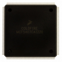
MCF5407CAI220 Freescale Semiconductor, MCF5407CAI220 Datasheet - Page 422

MCF5407CAI220
Manufacturer Part Number
MCF5407CAI220
Description
IC MPU 32B 220MHZ COLDF 208-FQFP
Manufacturer
Freescale Semiconductor
Series
MCF540xr
Specifications of MCF5407CAI220
Core Processor
Coldfire V4
Core Size
32-Bit
Speed
220MHz
Connectivity
EBI/EMI, I²C, UART/USART
Peripherals
DMA, WDT
Number Of I /o
16
Program Memory Type
ROMless
Ram Size
4K x 8
Voltage - Supply (vcc/vdd)
1.65 V ~ 3.6 V
Oscillator Type
External
Operating Temperature
-40°C ~ 85°C
Package / Case
208-FQFP
Processor Series
MCF540x
Core
ColdFire V4
Data Bus Width
32 bit
Program Memory Size
8 KB
Data Ram Size
4 KB
Maximum Clock Frequency
162 MHz
Number Of Programmable I/os
16
Operating Supply Voltage
1.8 V to 3.3 V
Mounting Style
SMD/SMT
3rd Party Development Tools
JLINK-CF-BDM26, EWCF
Cpu Speed
220MHz
Embedded Interface Type
I2C, UART
Digital Ic Case Style
FQFP
No. Of Pins
208
Supply Voltage Range
3.3V
Rohs Compliant
Yes
For Use With
M5407C3 - KIT EVAL FOR MCF5407 W/ETHERNET
Lead Free Status / RoHS Status
Lead free / RoHS Compliant
Eeprom Size
-
Program Memory Size
-
Data Converters
-
Lead Free Status / Rohs Status
Lead free / RoHS Compliant
Available stocks
Company
Part Number
Manufacturer
Quantity
Price
Company:
Part Number:
MCF5407CAI220
Manufacturer:
Freescale
Quantity:
789
Company:
Part Number:
MCF5407CAI220
Manufacturer:
Freescale Semiconductor
Quantity:
10 000
- Current page: 422 of 546
- Download datasheet (7Mb)
DRAM Controller Signals
ROM to be selected at any defined address space. Port size and termination (internal vs.
external) for boot CS0 are configured by the levels on D[7:5,3] on the rising edge of RSTI,
as described in Section 17.5.5.1, “D[7:5,3]—Boot Chip-Select (CS0) Configuration.”
The chip-select implementation is described in Chapter 10, “Chip-Select Module.”
17.6.2 Byte Enables/Byte Write Enables (BE[3:0]/BWE[3:0])
The four byte enables are multiplexed with the MCF5407 byte-write-enable signals. Each
pin can be individually programmed through the chip-select control registers (CSCRs). For
each chip select, assertion of byte enables for reads and byte-write enables for write cycles
can be programmed. Alternatively, users can program byte-write enables to assert on writes
and no byte enable assertion for read transfers.
17.6.3 Output Enable (OE)
The output enable (OE) signal is sent to the interfacing memory and/or peripheral to enable
a read transfer. OE is asserted only when a chip select matches the current address decode.
17.7 DRAM Controller Signals
The DRAM signals in the following sections interface to external DRAM. DRAM with
widths of 8, 16, and 32 bits are supported and can access as much as 512 Mbytes of DRAM.
17.7.1 Row Address Strobes (RAS[1:0])
The row address strobes (RAS[1:0]) interface to RAS inputs on industry-standard
ADRAMs. When SDRAMs are used, these signals interface to the chip-select lines of the
SDRAMs within a memory block. Thus, there is one RAS line for each memory block
(because the MCF5407 supports only two memory blocks).
17.7.2 Column Address Strobes (CAS[3:0])
The column address strobes (CAS[3:0]) interface to CAS inputs on industry-standard
DRAMs. These provide CAS for a given ADRAM block. When SDRAMs are used, CAS
signals control the byte enables for standard SDRAMs (referred to as DQMx). CAS3
accesses the LSB and CAS0 accesses the MSB of data.
17.7.3 DRAM Write (DRAMW)
The DRAM write signal (DRAMW) is asserted to signify that a DRAM write cycle is
underway. A read bus cycle is indicated by the negation of DRAMW.
MCF5407 User’s Manual
17-16
Related parts for MCF5407CAI220
Image
Part Number
Description
Manufacturer
Datasheet
Request
R
Part Number:
Description:
Mcf5407 Coldfire Integrated Microprocessor User
Manufacturer:
Freescale Semiconductor, Inc
Datasheet:
Part Number:
Description:
Manufacturer:
Freescale Semiconductor, Inc
Datasheet:
Part Number:
Description:
Manufacturer:
Freescale Semiconductor, Inc
Datasheet:
Part Number:
Description:
Manufacturer:
Freescale Semiconductor, Inc
Datasheet:
Part Number:
Description:
Manufacturer:
Freescale Semiconductor, Inc
Datasheet:
Part Number:
Description:
Manufacturer:
Freescale Semiconductor, Inc
Datasheet:
Part Number:
Description:
Manufacturer:
Freescale Semiconductor, Inc
Datasheet:
Part Number:
Description:
Manufacturer:
Freescale Semiconductor, Inc
Datasheet:
Part Number:
Description:
Manufacturer:
Freescale Semiconductor, Inc
Datasheet:
Part Number:
Description:
Manufacturer:
Freescale Semiconductor, Inc
Datasheet:
Part Number:
Description:
Manufacturer:
Freescale Semiconductor, Inc
Datasheet:
Part Number:
Description:
Manufacturer:
Freescale Semiconductor, Inc
Datasheet:
Part Number:
Description:
Manufacturer:
Freescale Semiconductor, Inc
Datasheet:
Part Number:
Description:
Manufacturer:
Freescale Semiconductor, Inc
Datasheet:
Part Number:
Description:
Manufacturer:
Freescale Semiconductor, Inc
Datasheet:


