DF2398TE20V Renesas Electronics America, DF2398TE20V Datasheet - Page 688
DF2398TE20V
Manufacturer Part Number
DF2398TE20V
Description
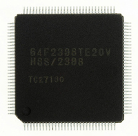
IC H8S MCU FLASH 256K 120TQFP
Manufacturer
Renesas Electronics America
Series
H8® H8S/2300r
Specifications of DF2398TE20V
Core Processor
H8S/2000
Core Size
16-Bit
Speed
20MHz
Connectivity
SCI, SmartCard
Peripherals
DMA, POR, PWM, WDT
Number Of I /o
87
Program Memory Size
256KB (256K x 8)
Program Memory Type
FLASH
Ram Size
8K x 8
Voltage - Supply (vcc/vdd)
4.5 V ~ 5.5 V
Data Converters
A/D 8x10b; D/A 2x8b
Oscillator Type
Internal
Operating Temperature
-20°C ~ 75°C
Package / Case
120-TQFP, 120-VQFP
For Use With
YR0K42378FC000BA - KIT EVAL FOR H8S/2378
Lead Free Status / RoHS Status
Lead free / RoHS Compliant
Eeprom Size
-
Other names
HD64F2398TE20V
Available stocks
Company
Part Number
Manufacturer
Quantity
Price
Company:

Part Number:
DF2398TE20V
Manufacturer:
Renesas Electronics America
Quantity:
10 000


19.22.10 Notes on Memory Programming
Notes: 1. The flash memory is initially in the erased state when the device is shipped by Renesas Technology. For other
19.23
Precautions concerning the use of on-board programming mode, the RAM emulation function, and programmer mode are
summarized below.
Use the specified voltages and timing for programming and erasing: Applied voltages in excess of the rating can
permanently damage the device. Use a PROM programmer that supports the Renesas Technology microcomputer device
type with 256-kbyte on-chip flash memory (FZTAT256V5A).
Do not select the HN27C4096 setting for the PROM programmer, and only use the specified socket adapter. Failure to
observe these points may result in damage to the device.
Powering on and off: When applying or disconnecting V
hardware protection state.
The power-on and power-off timing requirements should also be satisfied in the event of a power failure and subsequent
recovery.
Use the recommended algorithm when programming and erasing flash memory: The recommended algorithm
enables programming and erasing to be carried out without subjecting the device to voltage stress or sacrificing program
data reliability. When setting the P or E bit in FLMCR1, the watchdog timer should be set beforehand as a precaution
against program runaway, etc.
Do not set or clear the SWE bit during execution of a program in flash memory: Wait for at least 100 s after
clearing the SWE bit before executing a program or reading data in flash memory. When the SWE bit is set, data in flash
memory can be rewritten, but when SWE = 1, flash memory can only be read in program-verify or erase-verify mode.
Access flash memory only for verify operations (verification during programming/erasing). Also, do not clear the SWE bit
during programming, erasing, or verifying.
Similarly, when using the RAM emulation function the SWE bit must be cleared before executing a program or reading
data in flash memory.
However, the RAM area overlapping flash memory space can be read and written to regardless of whether the SWE bit is
set or cleared.
Do not use interrupts while flash memory is being programmed or erased: When flash memory is programmed or
erased, all interrupt requests, including NMI, should be disabled to give priority to program/erase operations.
Do not perform additional programming. Erase the memory before reprogramming: In on-board programming,
perform only one programming operation on a 128-byte programming unit block. In programmer mode, too, perform only
Rev.6.00 Oct.28.2004 page 658 of 1016
REJ09B0138-0600H
When programming addresses which have previously been programmed, carry out auto-erasing before auto-
programming.
When performing programming using PROM mode on a chip that has been programmed/erased in an on-board
programming mode, auto-erasing is recommended before carrying out auto-programming.
2. Auto-programming should be performed once only on the same address block. Additional programming cannot
Flash Memory Programming and Erasing Precautions
chips for which the erasure history is unknown, it is recommended that auto-erasing be executed to check and
supplement the initialization (erase) level.
be carried out on address blocks that have already been programmed.
CC
power, fix the RES pin low and place the flash memory in the
Related parts for DF2398TE20V
Image
Part Number
Description
Manufacturer
Datasheet
Request
R

Part Number:
Description:
CONN PLUG 12POS DUAL 0.5MM SMD
Manufacturer:
Hirose Electric Co Ltd
Datasheet:
Part Number:
Description:
CONN PLUG 18POS DUAL 0.5MM SMD
Manufacturer:
Hirose Electric Co Ltd
Datasheet:
Part Number:
Description:
CONN PLUG 14POS DUAL 0.5MM SMD
Manufacturer:
Hirose Electric Co Ltd
Datasheet:
Part Number:
Description:
CONN RECEPT 20POS DUAL 0.5MM SMD
Manufacturer:
Hirose Electric Co Ltd
Datasheet:
Part Number:
Description:
CONN PLUG 16POS DUAL 0.5MM SMD
Manufacturer:
Hirose Electric Co Ltd
Datasheet:
Part Number:
Description:
CONN RECEPT 16POS DUAL 0.5MM SMD
Manufacturer:
Hirose Electric Co Ltd
Datasheet:
Part Number:
Description:
CONN PLUG 20POS DUAL 0.5MM SMD
Manufacturer:
Hirose Electric Co Ltd
Datasheet:
Part Number:
Description:
CONN PLUG 30POS DUAL 0.5MM SMD
Manufacturer:
Hirose Electric Co Ltd
Datasheet:
Part Number:
Description:
CONN RECEPT 30POS DUAL 0.5MM SMD
Manufacturer:
Hirose Electric Co Ltd
Datasheet:
Part Number:
Description:
CONN PLUG 40POS DUAL 0.5MM SMD
Manufacturer:
Hirose Electric Co Ltd
Datasheet:

Part Number:
Description:
KIT STARTER FOR M16C/29
Manufacturer:
Renesas Electronics America
Datasheet:

Part Number:
Description:
KIT STARTER FOR R8C/2D
Manufacturer:
Renesas Electronics America
Datasheet:

Part Number:
Description:
R0K33062P STARTER KIT
Manufacturer:
Renesas Electronics America
Datasheet:

Part Number:
Description:
KIT STARTER FOR R8C/23 E8A
Manufacturer:
Renesas Electronics America
Datasheet:

Part Number:
Description:
KIT STARTER FOR R8C/25
Manufacturer:
Renesas Electronics America
Datasheet: