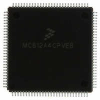
MC812A4CPVE8 Freescale Semiconductor, MC812A4CPVE8 Datasheet - Page 212

MC812A4CPVE8
Manufacturer Part Number
MC812A4CPVE8
Description
IC MCU 16BIT EEPROM 4K 112-LQFP
Manufacturer
Freescale Semiconductor
Series
HC12r
Datasheet
1.MC812A4CPVE8.pdf
(242 pages)
Specifications of MC812A4CPVE8
Core Processor
CPU12
Core Size
16-Bit
Speed
8MHz
Connectivity
SCI, SPI
Peripherals
POR, WDT
Number Of I /o
83
Program Memory Size
4KB (4K x 8)
Program Memory Type
EEPROM
Ram Size
1K x 8
Voltage - Supply (vcc/vdd)
4.5 V ~ 5.5 V
Data Converters
A/D 8x8b
Oscillator Type
Internal
Operating Temperature
-40°C ~ 85°C
Package / Case
112-LQFP
Processor Series
HC812A
Core
HC12
Data Bus Width
16 bit
Data Ram Size
1 KB
Interface Type
SCI, SPI
Maximum Clock Frequency
8 MHz
Number Of Programmable I/os
91
Number Of Timers
8
Maximum Operating Temperature
+ 85 C
Mounting Style
SMD/SMT
Minimum Operating Temperature
- 40 C
On-chip Adc
8 bit, 8 Channel
Controller Family/series
68HC12
No. Of I/o's
91
Eeprom Memory Size
4KB
Ram Memory Size
1KB
Cpu Speed
8MHz
No. Of Timers
1
Rohs Compliant
Yes
Lead Free Status / RoHS Status
Lead free / RoHS Compliant
Eeprom Size
-
Lead Free Status / Rohs Status
Details
Available stocks
Company
Part Number
Manufacturer
Quantity
Price
Company:
Part Number:
MC812A4CPVE8
Manufacturer:
MOTOLOLA
Quantity:
672
Company:
Part Number:
MC812A4CPVE8
Manufacturer:
Freescale Semiconductor
Quantity:
10 000
Part Number:
MC812A4CPVE8
Manufacturer:
NXP/恩智浦
Quantity:
20 000
Company:
Part Number:
MC812A4CPVE80
Manufacturer:
SHARP
Quantity:
5 510
Development Support
Program information is fetched a few cycles before it is used by the CPU. To monitor cycle-by-cycle CPU
activity, it is necessary to externally reconstruct what is happening in the instruction queue. Internally, the
MCU only needs to buffer the data from program fetches. For system debug, it is necessary to keep the
data and its associated address in the reconstructed instruction queue. The raw signals required for
reconstruction of the queue are ADDR, DATA, R/W, ECLK, and status signals IPIPE[1:0].
The instruction queue consists of two 16-bit queue stages and a holding latch on the input of the first
stage. To advance the queue means to move the word in the first stage to the second stage and move
the word from either the holding latch or the data bus input buffer into the first stage. To start even (or
odd) instruction means to execute the opcode in the high-order (or low-order) byte of the second stage of
the instruction queue.
17.3 Background Debug Mode (BDM)
Background debug mode (BDM) is used for:
BDM is implemented in on-chip hardware and provides a full set of debug options.
Because BDM control logic does not reside in the CPU, BDM hardware commands can be executed while
the CPU is operating normally. The control logic generally uses CPU dead cycles to execute these
commands, but can steal cycles from the CPU when necessary. Other BDM commands are firmware
based and require the CPU to be in active background mode for execution. While BDM is active, the CPU
executes a firmware program located in a small on-chip ROM that is available in the standard 64-Kbyte
memory map only while BDM is active.
The BDM control logic communicates with an external host development system serially, via the BKGD
pin. This single-wire approach minimizes the number of pins needed for development support.
17.3.1 BDM Serial Interface
The BDM serial interface requires the external controller to generate a falling edge on the BKGD pin to
indicate the start of each bit time. The external controller provides this falling edge whether data is
transmitted or received.
BKGD is a pseudo-open-drain pin that can be driven either by an external controller or by the MCU. Data
is transferred MSB first at 16 E-clock cycles per bit (nominal speed). The interface times out if 512 E-clock
cycles occur between falling edges from the host. The hardware clears the command register when this
timeout occurs.
The BKGD pin can receive a high or low level or transmit a high or low level. The following diagrams show
timing for each of these cases. Interface timing is synchronous to MCU clocks but asynchronous to the
external host. The internal clock signal is shown for reference in counting cycles.
212
•
•
•
•
System development
In-circuit testing
Field testing
Programming
MC68HC812A4 Data Sheet, Rev. 7
Freescale Semiconductor


