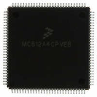
MC812A4CPVE8 Freescale Semiconductor, MC812A4CPVE8 Datasheet - Page 167

MC812A4CPVE8
Manufacturer Part Number
MC812A4CPVE8
Description
IC MCU 16BIT EEPROM 4K 112-LQFP
Manufacturer
Freescale Semiconductor
Series
HC12r
Datasheet
1.MC812A4CPVE8.pdf
(242 pages)
Specifications of MC812A4CPVE8
Core Processor
CPU12
Core Size
16-Bit
Speed
8MHz
Connectivity
SCI, SPI
Peripherals
POR, WDT
Number Of I /o
83
Program Memory Size
4KB (4K x 8)
Program Memory Type
EEPROM
Ram Size
1K x 8
Voltage - Supply (vcc/vdd)
4.5 V ~ 5.5 V
Data Converters
A/D 8x8b
Oscillator Type
Internal
Operating Temperature
-40°C ~ 85°C
Package / Case
112-LQFP
Processor Series
HC812A
Core
HC12
Data Bus Width
16 bit
Data Ram Size
1 KB
Interface Type
SCI, SPI
Maximum Clock Frequency
8 MHz
Number Of Programmable I/os
91
Number Of Timers
8
Maximum Operating Temperature
+ 85 C
Mounting Style
SMD/SMT
Minimum Operating Temperature
- 40 C
On-chip Adc
8 bit, 8 Channel
Controller Family/series
68HC12
No. Of I/o's
91
Eeprom Memory Size
4KB
Ram Memory Size
1KB
Cpu Speed
8MHz
No. Of Timers
1
Rohs Compliant
Yes
Lead Free Status / RoHS Status
Lead free / RoHS Compliant
Eeprom Size
-
Lead Free Status / Rohs Status
Details
Available stocks
Company
Part Number
Manufacturer
Quantity
Price
Company:
Part Number:
MC812A4CPVE8
Manufacturer:
MOTOLOLA
Quantity:
672
Company:
Part Number:
MC812A4CPVE8
Manufacturer:
Freescale Semiconductor
Quantity:
10 000
Part Number:
MC812A4CPVE8
Manufacturer:
NXP/恩智浦
Quantity:
20 000
Company:
Part Number:
MC812A4CPVE80
Manufacturer:
SHARP
Quantity:
5 510
Enable single-wire operation by setting the LOOPS bit and the receiver source bit, RSRC, in SCI control
register 1 (SCCR1). Setting the LOOPS bit disables the path from the RXD pin to the receiver. Setting the
RSRC bit connects the receiver input to the output of the TXD pin driver. Both the transmitter and receiver
must be enabled (TE = 1 and RE = 1).
The wired-OR mode select bit, WOMS, configures the TXD pin for full CMOS drive or for open-drain drive.
WOMS controls the TXD pin in both normal operation and in single-wire operation. When WOMS is set,
the data direction bit for the TXD pin does not have to be cleared for TXD to receive data.
14.5.6 Loop Operation
In loop operation, the transmitter output goes to the receiver input. The RXD pin is disconnected from the
SCI and is available as a general-purpose I/O pin.
Setting the data direction bit for the TXD pin connects the transmitter output to the TXD pin. Clearing the
data direction bit disconnects the transmitter output from the TXD pin.
Enable loop operation by setting the LOOPS bit and clearing the RSRC bit in SCI control register 1
(SCCR1). Setting the LOOPS bit disables the path from the RXD pin to the receiver. Clearing the RSRC
bit connects the transmitter output to the receiver input. Both the transmitter and receiver must be enabled
(TE = 1 and RE = 1).
The wired-OR mode select bit, WOMS, configures the TXD pin for full CMOS drive or for open-drain drive.
WOMS controls the TXD pin in both normal operation and in loop operation.
Freescale Semiconductor
DDRS BIT = 1
DDRS BIT = 0
Figure 14-16. Loop Operation (LOOP = 1 and RSRC = 0)
TRANSMITTER
TRANSMITTER
RECEIVER
RECEIVER
MC68HC812A4 Data Sheet, Rev. 7
H
WOMS
WOMS
TXD
RXD
TXD
RXD
GENERAL-
PURPOSE I/O
GENERAL-
PURPOSE I/O
Functional Description
167


