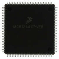
MC812A4CPVE8 Freescale Semiconductor, MC812A4CPVE8 Datasheet - Page 186

MC812A4CPVE8
Manufacturer Part Number
MC812A4CPVE8
Description
IC MCU 16BIT EEPROM 4K 112-LQFP
Manufacturer
Freescale Semiconductor
Series
HC12r
Datasheet
1.MC812A4CPVE8.pdf
(242 pages)
Specifications of MC812A4CPVE8
Core Processor
CPU12
Core Size
16-Bit
Speed
8MHz
Connectivity
SCI, SPI
Peripherals
POR, WDT
Number Of I /o
83
Program Memory Size
4KB (4K x 8)
Program Memory Type
EEPROM
Ram Size
1K x 8
Voltage - Supply (vcc/vdd)
4.5 V ~ 5.5 V
Data Converters
A/D 8x8b
Oscillator Type
Internal
Operating Temperature
-40°C ~ 85°C
Package / Case
112-LQFP
Processor Series
HC812A
Core
HC12
Data Bus Width
16 bit
Data Ram Size
1 KB
Interface Type
SCI, SPI
Maximum Clock Frequency
8 MHz
Number Of Programmable I/os
91
Number Of Timers
8
Maximum Operating Temperature
+ 85 C
Mounting Style
SMD/SMT
Minimum Operating Temperature
- 40 C
On-chip Adc
8 bit, 8 Channel
Controller Family/series
68HC12
No. Of I/o's
91
Eeprom Memory Size
4KB
Ram Memory Size
1KB
Cpu Speed
8MHz
No. Of Timers
1
Rohs Compliant
Yes
Lead Free Status / RoHS Status
Lead free / RoHS Compliant
Eeprom Size
-
Lead Free Status / Rohs Status
Details
Available stocks
Company
Part Number
Manufacturer
Quantity
Price
Company:
Part Number:
MC812A4CPVE8
Manufacturer:
MOTOLOLA
Quantity:
672
Company:
Part Number:
MC812A4CPVE8
Manufacturer:
Freescale Semiconductor
Quantity:
10 000
Part Number:
MC812A4CPVE8
Manufacturer:
NXP/恩智浦
Quantity:
20 000
Company:
Part Number:
MC812A4CPVE80
Manufacturer:
SHARP
Quantity:
5 510
Serial Peripheral Interface (SPI)
15.6 SPI Register Descriptions and Reset Initialization
This section describes the SPI registers and reset initialization.
15.6.1 SPI Control Register 1
Read: Anytime
Write: Anytime
SPIE — SPI Interrupt Enable Bit
SPE — SPI Enable Bit
SWOM — Port S Wired-OR Mode Bit
MSTR — Master Mode Bit
CPOL — Clock Polarity Bit
CPHA — Clock Phase Bit
186
SPIE enables the SPIF and MODF flags to generate interrupt requests.
Setting the SPE bit enables the SPI and configures port S pins 7–4 for SPI functions. Clearing SPE
puts the SPI in a disabled, low-power state.
SWOM disables the pullup devices on port S pins 7–4 so that they become open-drain outputs.
MSTR selects master mode operation or slave mode operation.
CPOL determines the logic state of the serial clock pin between transmissions. See
Figure
CPHA determines whether transmission begins on the falling edge of the SS pin or on the first edge
of the serial clock. See
1 = SPIF and MODF interrupt requests enabled
0 = SPIF and MODF interrupt requests disabled
1 = SPI enabled
0 = SPI disabled
1 = Open-drain port S pin 7–4 outputs
0 = Normal push-pull port S pin 7–4 outputs
1 = Master mode
0 = Slave mode
1 = Active-high SCK
0 = Active-low SCK
1 = Transmission at first SCK edge
0 = Transmission at falling SS edge
15-6.
Address: $00D0
When the MODF flag is set, SPE always reads as logic 0. Writing to SPI
control register 1 is part of the mode fault recovery sequence.
Reset:
Read:
Write:
SPIE
Bit 7
0
Figure 15-4
Figure 15-9. SPI Control Register 1 (SP0CR1)
SPE
6
0
MC68HC812A4 Data Sheet, Rev. 7
and
SWOM
5
0
Figure
MSTR
NOTE
15-6.
4
0
CPOL
3
0
CPHA
2
1
SSOE
1
0
Freescale Semiconductor
LSBF
Bit 0
0
Figure 15-4
and


