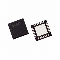
C8051F321-GM Silicon Laboratories Inc, C8051F321-GM Datasheet - Page 40

C8051F321-GM
Manufacturer Part Number
C8051F321-GM
Description
IC 8051 MCU 16K FLASH 28MLP
Manufacturer
Silicon Laboratories Inc
Series
C8051F32xr
Datasheets
1.C8051F320-TB.pdf
(250 pages)
2.C8051F321-GMR.pdf
(2 pages)
3.C8051F321-GM.pdf
(256 pages)
Specifications of C8051F321-GM
Program Memory Type
FLASH
Program Memory Size
16KB (16K x 8)
Package / Case
28-VQFN Exposed Pad, 28-HVQFN, 28-SQFN, 28-DHVQFN
Core Processor
8051
Core Size
8-Bit
Speed
25MHz
Connectivity
SMBus (2-Wire/I²C), SPI, UART/USART, USB
Peripherals
Brown-out Detect/Reset, POR, PWM, Temp Sensor, WDT
Number Of I /o
21
Ram Size
2.25K x 8
Voltage - Supply (vcc/vdd)
2.7 V ~ 3.6 V
Data Converters
A/D 13x10b
Oscillator Type
Internal
Operating Temperature
-40°C ~ 85°C
Processor Series
C8051F3x
Core
8051
Data Bus Width
8 bit
Data Ram Size
2.25 KB
Interface Type
I2C/SMBus/SPI/UART/USB
Maximum Clock Frequency
25 MHz
Number Of Programmable I/os
21
Number Of Timers
4
Operating Supply Voltage
2.7 V to 3.6 V
Maximum Operating Temperature
+ 85 C
Mounting Style
SMD/SMT
3rd Party Development Tools
PK51, CA51, A51, ULINK2
Development Tools By Supplier
C8051F320DK
Minimum Operating Temperature
- 40 C
On-chip Adc
13-ch x 10-bit or 17-ch x 10-bit
No. Of I/o's
21
Ram Memory Size
1280Byte
Cpu Speed
25MHz
No. Of Timers
4
Rohs Compliant
Yes
Lead Free Status / RoHS Status
Lead free / RoHS Compliant
For Use With
336-1480 - DAUGHTER CARD TOOLSTCK C8051F321770-1006 - ISP 4PORT FOR SILABS C8051F MCU336-1449 - ADAPTER PROGRAM TOOLSTICK F321336-1260 - DEV KIT FOR C8051F320/F321
Eeprom Size
-
Lead Free Status / Rohs Status
Lead free / RoHS Compliant
Other names
336-1261
Available stocks
Company
Part Number
Manufacturer
Quantity
Price
Company:
Part Number:
C8051F321-GM
Manufacturer:
SiliconL
Quantity:
4 364
Part Number:
C8051F321-GM
Manufacturer:
SILICON LABS/芯科
Quantity:
20 000
Part Number:
C8051F321-GMR
Manufacturer:
SILICON LABS/芯科
Quantity:
20 000
C8051F320/1
5.1.
AMUX0 selects the positive and negative inputs to the ADC. Any of the following may be selected as the positive
input: P1.0-P3.0, the on-chip temperature sensor, or the positive power supply (VDD). Any of the following may be
selected as the negative input: P1.0-P3.0, VREF, or GND. When GND is selected as the negative input, ADC0
operates in Single-ended Mode; all other times, ADC0 operates in Differential Mode. The ADC0 input channels
are selected in the AMX0P and AMX0N registers as described in Figure 5.5 and Figure 5.6.
The conversion code format differs between Single-ended and Differential modes. The registers ADC0H and ADC0L
contain the high and low bytes of the output conversion code from the ADC at the completion of each conversion.
Data can be right-justified or left-justified, depending on the setting of the AD0LJST bit (ADC0CN.0). When in Sin-
gle-ended Mode, conversion codes are represented as 10-bit unsigned integers. Inputs are measured from ‘0’ to
VREF * 1023/1024. Example codes are shown below for both right-justified and left-justified data. Unused bits in the
ADC0H and ADC0L registers are set to ‘0’.
When in Differential Mode, conversion codes are represented as 10-bit signed 2’s complement numbers. Inputs are
measured from -VREF to VREF * 511/512. Example codes are shown below for both right-justified and left-justified
data. For right-justified data, the unused MSBs of ADC0H are a sign-extension of the data word. For left-justified
data, the unused LSBs in the ADC0L register are set to ‘0’.
Important Note About ADC0 Input Configuration: Port pins selected as ADC0 inputs should be configured as
analog inputs, and should be skipped by the Digital Crossbar. To configure a Port pin for analog input, set to ‘0’ the
corresponding bit in register PnMDIN (for n = 0,1,2,3). To force the Crossbar to skip a Port pin, set to ‘1’ the corre-
sponding bit in register PnSKIP (for n = 0,1,2). See
configuration details.
40
VREF * 1023/1024
VREF * 512/1024
VREF * 256/1024
-VREF * 256/512
VREF * 511/512
VREF * 256/512
(Single-Ended)
Input Voltage
Input Voltage
(Differential)
- VREF
Analog Multiplexer
0
0
Right-Justified ADC0H:ADC0L
Right-Justified ADC0H:ADC0L
(AD0LJST = 0)
(AD0LJST = 0)
0xFE00
0x01FF
0xFF00
0x03FF
0x0100
0x0000
0x0200
0x0100
0x0000
Section “14. Port Input/Output” on page 127
Rev. 1.1
Left-Justified ADC0H:ADC0L
Left-Justified ADC0H:ADC0L
(AD0LJST = 1)
(AD0LJST = 1)
0xFFC0
0x7FC0
0x8000
0x4000
0x0000
0xC000
0x4000
0x0000
0x8000
for more Port I/O


