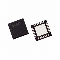
C8051F321-GM Silicon Laboratories Inc, C8051F321-GM Datasheet - Page 177

C8051F321-GM
Manufacturer Part Number
C8051F321-GM
Description
IC 8051 MCU 16K FLASH 28MLP
Manufacturer
Silicon Laboratories Inc
Series
C8051F32xr
Datasheets
1.C8051F320-TB.pdf
(250 pages)
2.C8051F321-GMR.pdf
(2 pages)
3.C8051F321-GM.pdf
(256 pages)
Specifications of C8051F321-GM
Program Memory Type
FLASH
Program Memory Size
16KB (16K x 8)
Package / Case
28-VQFN Exposed Pad, 28-HVQFN, 28-SQFN, 28-DHVQFN
Core Processor
8051
Core Size
8-Bit
Speed
25MHz
Connectivity
SMBus (2-Wire/I²C), SPI, UART/USART, USB
Peripherals
Brown-out Detect/Reset, POR, PWM, Temp Sensor, WDT
Number Of I /o
21
Ram Size
2.25K x 8
Voltage - Supply (vcc/vdd)
2.7 V ~ 3.6 V
Data Converters
A/D 13x10b
Oscillator Type
Internal
Operating Temperature
-40°C ~ 85°C
Processor Series
C8051F3x
Core
8051
Data Bus Width
8 bit
Data Ram Size
2.25 KB
Interface Type
I2C/SMBus/SPI/UART/USB
Maximum Clock Frequency
25 MHz
Number Of Programmable I/os
21
Number Of Timers
4
Operating Supply Voltage
2.7 V to 3.6 V
Maximum Operating Temperature
+ 85 C
Mounting Style
SMD/SMT
3rd Party Development Tools
PK51, CA51, A51, ULINK2
Development Tools By Supplier
C8051F320DK
Minimum Operating Temperature
- 40 C
On-chip Adc
13-ch x 10-bit or 17-ch x 10-bit
No. Of I/o's
21
Ram Memory Size
1280Byte
Cpu Speed
25MHz
No. Of Timers
4
Rohs Compliant
Yes
Lead Free Status / RoHS Status
Lead free / RoHS Compliant
For Use With
336-1480 - DAUGHTER CARD TOOLSTCK C8051F321770-1006 - ISP 4PORT FOR SILABS C8051F MCU336-1449 - ADAPTER PROGRAM TOOLSTICK F321336-1260 - DEV KIT FOR C8051F320/F321
Eeprom Size
-
Lead Free Status / Rohs Status
Lead free / RoHS Compliant
Other names
336-1261
Available stocks
Company
Part Number
Manufacturer
Quantity
Price
Company:
Part Number:
C8051F321-GM
Manufacturer:
SiliconL
Quantity:
4 364
Part Number:
C8051F321-GM
Manufacturer:
SILICON LABS/芯科
Quantity:
20 000
Part Number:
C8051F321-GMR
Manufacturer:
SILICON LABS/芯科
Quantity:
20 000
C8051F320/1
16.3. SMBus Operation
Two types of data transfers are possible: data transfers from a master transmitter to an addressed slave receiver
(WRITE), and data transfers from an addressed slave transmitter to a master receiver (READ). The master device ini-
tiates both types of data transfers and provides the serial clock pulses on SCL. The SMBus interface may operate as a
master or a slave, and multiple master devices on the same bus are supported. If two or more masters attempt to ini-
tiate a data transfer simultaneously, an arbitration scheme is employed with a single master always winning the arbi-
tration. Note that it is not necessary to specify one device as the Master in a system; any device who transmits a
START and a slave address becomes the master for the duration of that transfer.
A typical SMBus transaction consists of a START condition followed by an address byte (Bits7-1: 7-bit slave
address; Bit0: R/W direction bit), one or more bytes of data, and a STOP condition. Each byte that is received (by a
master or slave) must be acknowledged (ACK) with a low SDA during a high SCL (see Figure 16.3). If the receiving
device does not ACK, the transmitting device will read a NACK (not acknowledge), which is a high SDA during a
high SCL.
The direction bit (R/W) occupies the least-significant bit position of the address byte. The direction bit is set to logic
1 to indicate a "READ" operation and cleared to logic 0 to indicate a "WRITE" operation.
All transactions are initiated by a master, with one or more addressed slave devices as the target. The master gener-
ates the START condition and then transmits the slave address and direction bit. If the transaction is a WRITE opera-
tion from the master to the slave, the master transmits the data a byte at a time waiting for an ACK from the slave at
the end of each byte. For READ operations, the slave transmits the data waiting for an ACK from the master at the
end of each byte. At the end of the data transfer, the master generates a STOP condition to terminate the transaction
and free the bus. Figure 16.3 illustrates a typical SMBus transaction.
Figure 16.3. SMBus Transaction
SCL
SDA
SLA6
SLA5-0
R/W
D7
D6-0
START
Slave Address + R/W
ACK
Data Byte
NACK
STOP
16.3.1. Arbitration
A master may start a transfer only if the bus is free. The bus is free after a STOP condition or after the SCL and SDA
lines remain high for a specified time (see
Section “16.3.4. SCL High (SMBus Free) Timeout” on page
178). In the
event that two or more devices attempt to begin a transfer at the same time, an arbitration scheme is employed to
force one master to give up the bus. The master devices continue transmitting until one attempts a HIGH while the
other transmits a LOW. Since the bus is open-drain, the bus will be pulled LOW. The master attempting the HIGH
will detect a LOW SDA and lose the arbitration. The winning master continues its transmission without interruption;
the losing master becomes a slave and receives the rest of the transfer if addressed. This arbitration scheme is non-
destructive: one device always wins, and no data is lost.
Rev. 1.1
177


