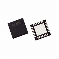
C8051F321-GM Silicon Laboratories Inc, C8051F321-GM Datasheet - Page 31

C8051F321-GM
Manufacturer Part Number
C8051F321-GM
Description
IC 8051 MCU 16K FLASH 28MLP
Manufacturer
Silicon Laboratories Inc
Series
C8051F32xr
Datasheets
1.C8051F320-TB.pdf
(250 pages)
2.C8051F321-GMR.pdf
(2 pages)
3.C8051F321-GM.pdf
(256 pages)
Specifications of C8051F321-GM
Program Memory Type
FLASH
Program Memory Size
16KB (16K x 8)
Package / Case
28-VQFN Exposed Pad, 28-HVQFN, 28-SQFN, 28-DHVQFN
Core Processor
8051
Core Size
8-Bit
Speed
25MHz
Connectivity
SMBus (2-Wire/I²C), SPI, UART/USART, USB
Peripherals
Brown-out Detect/Reset, POR, PWM, Temp Sensor, WDT
Number Of I /o
21
Ram Size
2.25K x 8
Voltage - Supply (vcc/vdd)
2.7 V ~ 3.6 V
Data Converters
A/D 13x10b
Oscillator Type
Internal
Operating Temperature
-40°C ~ 85°C
Processor Series
C8051F3x
Core
8051
Data Bus Width
8 bit
Data Ram Size
2.25 KB
Interface Type
I2C/SMBus/SPI/UART/USB
Maximum Clock Frequency
25 MHz
Number Of Programmable I/os
21
Number Of Timers
4
Operating Supply Voltage
2.7 V to 3.6 V
Maximum Operating Temperature
+ 85 C
Mounting Style
SMD/SMT
3rd Party Development Tools
PK51, CA51, A51, ULINK2
Development Tools By Supplier
C8051F320DK
Minimum Operating Temperature
- 40 C
On-chip Adc
13-ch x 10-bit or 17-ch x 10-bit
No. Of I/o's
21
Ram Memory Size
1280Byte
Cpu Speed
25MHz
No. Of Timers
4
Rohs Compliant
Yes
Lead Free Status / RoHS Status
Lead free / RoHS Compliant
For Use With
336-1480 - DAUGHTER CARD TOOLSTCK C8051F321770-1006 - ISP 4PORT FOR SILABS C8051F MCU336-1449 - ADAPTER PROGRAM TOOLSTICK F321336-1260 - DEV KIT FOR C8051F320/F321
Eeprom Size
-
Lead Free Status / Rohs Status
Lead free / RoHS Compliant
Other names
336-1261
Available stocks
Company
Part Number
Manufacturer
Quantity
Price
Company:
Part Number:
C8051F321-GM
Manufacturer:
SiliconL
Quantity:
4 364
Part Number:
C8051F321-GM
Manufacturer:
SILICON LABS/芯科
Quantity:
20 000
Part Number:
C8051F321-GMR
Manufacturer:
SILICON LABS/芯科
Quantity:
20 000
4.
XTAL1
XTAL2
REGIN
VBUS
Name
C2CK
/RST/
VDD
GND
P3.0/
P0.2/
P0.3/
C2D
P0.0
P0.1
P0.4
P0.5
D+
D-
PINOUT AND PACKAGE DEFINITIONS
‘F320
Pin Numbers
10
32
31
30
29
6
3
9
7
8
4
5
2
1
Table 4.1. Pin Definitions for the C8051F320/1
‘F321
10
28
27
26
25
6
3
9
7
8
4
5
2
1
Power In
Power In 5 V Regulator Input. This pin is the input to the on-chip voltage
A I/O or
Power
D I/O
D I/O
D I/O
D I/O
D I/O
D I/O
D I/O
D I/O
D I/O
D I/O
D I/O
D I/O
Type
D In
A In
D In
Out
Description
2.7-3.6 V Power Supply Voltage Input.
3.3 V Voltage Regulator Output. See
Ground.
Device Reset. Open-drain output of internal POR or VDD moni-
tor. An external source can initiate a system reset by driving this
pin low for at least 15 µs. See
Clock signal for the C2 Debug Interface.
Port 3.0. See
Bi-directional data signal for the C2 Debug Interface.
regulator.
VBUS Sense Input. This pin should be connected to the VBUS
signal of a USB network. A 5 V signal on this pin indicates a USB
network connection.
USB D+.
USB D-.
Port 0.0. See
Port 0.1. See
Port 0.2. See
External Clock Input. This pin is the external oscillator return for
a crystal or resonator. See
Port 0.3. See
External Clock Output. This pin is the excitation driver for an
external crystal or resonator, or an external clock input for CMOS,
capacitor, or RC oscillator configurations. See
Port 0.4. See
Port 0.5. See
Rev. 1.1
Section 14
Section 14
Section 14
Section 14
Section 14
Section 14
Section 14
for a complete description.
for a complete description.
for a complete description.
for a complete description.
for a complete description.
for a complete description.
for a complete description.
Section
Section
13.
Section
C8051F320/1
10.
8.
Section
13.
31


