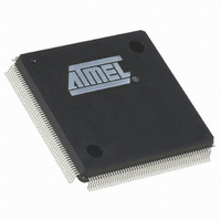
AT91RM9200-QU-002 Atmel, AT91RM9200-QU-002 Datasheet - Page 350

AT91RM9200-QU-002
Manufacturer Part Number
AT91RM9200-QU-002
Description
IC ARM9 MCU 208 PQFP
Manufacturer
Atmel
Series
AT91SAMr
Datasheets
1.AT91RM9200-EK.pdf
(41 pages)
2.AT91RM9200-QU-002.pdf
(701 pages)
3.AT91RM9200-QU-002.pdf
(38 pages)
Specifications of AT91RM9200-QU-002
Core Processor
ARM9
Core Size
16/32-Bit
Speed
180MHz
Connectivity
EBI/EMI, Ethernet, I²C, MMC, SPI, SSC, UART/USART, USB
Peripherals
POR
Number Of I /o
122
Program Memory Size
128KB (128K x 8)
Program Memory Type
ROM
Ram Size
48K x 8
Voltage - Supply (vcc/vdd)
1.65 V ~ 1.95 V
Oscillator Type
Internal
Operating Temperature
-40°C ~ 85°C
Package / Case
208-MQFP, 208-PQFP
Processor Series
AT91Rx
Core
ARM7TDMI
Data Bus Width
32 bit
Data Ram Size
16 KB
Interface Type
2-Wire, EBI, I2S, SPI, UART, USART
Maximum Clock Frequency
180 MHz
Number Of Programmable I/os
122
Number Of Timers
10 bit
Operating Supply Voltage
3 V to 3.6 V
Maximum Operating Temperature
+ 85 C
Mounting Style
SMD/SMT
3rd Party Development Tools
JTRACE-ARM-2M, MDK-ARM, RL-ARM, ULINK2
Development Tools By Supplier
AT91SAM-ICE, AT91-ISP, AT91RM9200-EK
Minimum Operating Temperature
- 40 C
Eeprom Memory
0 Bytes
Input Output
122
Interface
EBI/EMI, UART/USART
Ios
122
Memory Type
ROM
Number Of Bits
32
Package Type
208-pin PQFP
Programmable Memory
128K Bytes
Timers
3-16-bit
Voltage, Range
1.65-1.95 V
Cpu Family
91R
Device Core
ARM920T
Device Core Size
32b
Frequency (max)
180MHz
Total Internal Ram Size
16KB
# I/os (max)
122
Number Of Timers - General Purpose
6
Operating Supply Voltage (typ)
1.8/3.3V
Operating Supply Voltage (max)
1.95/3.6V
Operating Supply Voltage (min)
1.65/3V
Instruction Set Architecture
RISC
Operating Temp Range
-40C to 85C
Operating Temperature Classification
Industrial
Mounting
Surface Mount
Pin Count
208
For Use With
AT91SAM-ICE - EMULATOR FOR AT91 ARM7/ARM9
Lead Free Status / RoHS Status
Lead free / RoHS Compliant
Eeprom Size
-
Data Converters
-
Lead Free Status / Rohs Status
Lead free / RoHS Compliant
Available stocks
Company
Part Number
Manufacturer
Quantity
Price
Company:
Part Number:
AT91RM9200-QU-002
Manufacturer:
COSMO
Quantity:
12 000
Company:
Part Number:
AT91RM9200-QU-002
Manufacturer:
Atmel
Quantity:
1 680
Company:
Part Number:
AT91RM9200-QU-002
Manufacturer:
ATMEL
Quantity:
2 350
Part Number:
AT91RM9200-QU-002
Manufacturer:
ATMEL/爱特梅尔
Quantity:
20 000
Company:
Part Number:
AT91RM9200-QU-002-CQ
Manufacturer:
Atmel
Quantity:
3
- Current page: 350 of 701
- Download datasheet (10Mb)
27.4.5
27.4.6
27.4.7
350
AT91RM9200
Synchronous Data Output
Multi Drive Control (Open Drain)
Output Line Timings
be controlled by the PIO controller or assigned to a peripheral function. This enables configura-
tion of the I/O line prior to setting it to be managed by the PIO Controller.
Similarly, writing in PIO_SODR and PIO_CODR effects PIO_ODSR. This is important as it
defines the first level driven on the I/O line.
Using the write operations in PIO_SODR and PIO_CODR can require that several instructions
be executed in order to define values on several bits. Both clearing and setting I/O lines on an 8-
bit port, for example, cannot be done at the same time, and thus might limit the application cov-
ered by the PIO Controller.
To avoid these inconveniences, the PIO Controller features a Synchronous Data Output to clear
and set a number of I/O lines in a single write. This is performed by authorizing the writing of
PIO_ODSR (Output Data Status Register) from the register set PIO_OWER (Output Write
Enable Register), PIO_OWDR (Output Write Disable Register) and PIO_OWSR (Output Write
Status Register). The value of PIO_OWSR register is user-definable by writing in PIO_OWER
and PIO_OWDR. It is used by the PIO Controller as a PIO_ODSR write authorization mask.
Authorizing the write of PIO_ODSR on a user-definable number of bits is especially useful, as it
guarantees that the unauthorized bit will not be changed when writing it and thus avoids the
need of a time consuming read-modify-write operation.
After reset, the synchronous data output is disabled on all the I/O lines as PIO_OWSR resets at
0x0.
Each I/O can be independently programmed in Open Drain by using the Multi Drive feature. This
feature permits several drivers to be connected on the I/O line which is driven low only by each
device. An external pull-up resistor (or enabling of the internal one) is generally required to guar-
antee a high level on the line.
The Multi Drive feature is controlled by PIO_MDER (Multi-driver Enable Register) and
PIO_MDDR (Multi-driver Disable Register). The Multi Drive can be selected whether the I/O line
is controlled by the PIO controller or assigned to a peripheral function. PIO_MDSR (Multi-driver
Status Register) indicates the pins that are configured to support external drivers.
After reset, the Multi Drive feature is disabled on all pins, i.e. PIO_MDSR resets at value 0x0.
Figure 27-4
directly writing PIO_ODSR. This last case is valid only if the corresponding bit in PIO_OWSR is
set.
Figure 27-4
shows how the outputs are driven either by writing PIO_SODR or PIO_CODR, or by
also shows when the feedback in PIO_PDSR is available.
1768I–ATARM–09-Jul-09
Related parts for AT91RM9200-QU-002
Image
Part Number
Description
Manufacturer
Datasheet
Request
R

Part Number:
Description:
Manufacturer:
ATMEL Corporation
Datasheet:

Part Number:
Description:
IC ARM MCU 16BIT 128K 256BGA
Manufacturer:
Atmel
Datasheet:

Part Number:
Description:
IC ARM9 MCU 208 PQFP
Manufacturer:
Atmel
Datasheet:

Part Number:
Description:
DEVEL KIT
Manufacturer:
Atmel
Datasheet:

Part Number:
Description:
KIT DEVELOPMENT AT91RM9200
Manufacturer:
Atmel
Datasheet:

Part Number:
Description:
IC ARM9 MCU 256 BGA
Manufacturer:
Atmel
Datasheet:

Part Number:
Description:
IC ARM MCU 16BIT 128K 208PQFP
Manufacturer:
Atmel
Datasheet:

Part Number:
Description:
AT91RM9200 Development Kit
Manufacturer:
ATMEL Corporation
Datasheet:

Part Number:
Description:
DEV KIT FOR AVR/AVR32
Manufacturer:
Atmel
Datasheet:

Part Number:
Description:
INTERVAL AND WIPE/WASH WIPER CONTROL IC WITH DELAY
Manufacturer:
ATMEL Corporation
Datasheet:

Part Number:
Description:
Low-Voltage Voice-Switched IC for Hands-Free Operation
Manufacturer:
ATMEL Corporation
Datasheet:

Part Number:
Description:
MONOLITHIC INTEGRATED FEATUREPHONE CIRCUIT
Manufacturer:
ATMEL Corporation
Datasheet:

Part Number:
Description:
AM-FM Receiver IC U4255BM-M
Manufacturer:
ATMEL Corporation
Datasheet:


