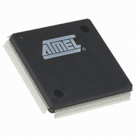
AT91RM9200-QU-002 Atmel, AT91RM9200-QU-002 Datasheet - Page 141

AT91RM9200-QU-002
Manufacturer Part Number
AT91RM9200-QU-002
Description
IC ARM9 MCU 208 PQFP
Manufacturer
Atmel
Series
AT91SAMr
Datasheets
1.AT91RM9200-EK.pdf
(41 pages)
2.AT91RM9200-QU-002.pdf
(701 pages)
3.AT91RM9200-QU-002.pdf
(38 pages)
Specifications of AT91RM9200-QU-002
Core Processor
ARM9
Core Size
16/32-Bit
Speed
180MHz
Connectivity
EBI/EMI, Ethernet, I²C, MMC, SPI, SSC, UART/USART, USB
Peripherals
POR
Number Of I /o
122
Program Memory Size
128KB (128K x 8)
Program Memory Type
ROM
Ram Size
48K x 8
Voltage - Supply (vcc/vdd)
1.65 V ~ 1.95 V
Oscillator Type
Internal
Operating Temperature
-40°C ~ 85°C
Package / Case
208-MQFP, 208-PQFP
Processor Series
AT91Rx
Core
ARM7TDMI
Data Bus Width
32 bit
Data Ram Size
16 KB
Interface Type
2-Wire, EBI, I2S, SPI, UART, USART
Maximum Clock Frequency
180 MHz
Number Of Programmable I/os
122
Number Of Timers
10 bit
Operating Supply Voltage
3 V to 3.6 V
Maximum Operating Temperature
+ 85 C
Mounting Style
SMD/SMT
3rd Party Development Tools
JTRACE-ARM-2M, MDK-ARM, RL-ARM, ULINK2
Development Tools By Supplier
AT91SAM-ICE, AT91-ISP, AT91RM9200-EK
Minimum Operating Temperature
- 40 C
Eeprom Memory
0 Bytes
Input Output
122
Interface
EBI/EMI, UART/USART
Ios
122
Memory Type
ROM
Number Of Bits
32
Package Type
208-pin PQFP
Programmable Memory
128K Bytes
Timers
3-16-bit
Voltage, Range
1.65-1.95 V
Cpu Family
91R
Device Core
ARM920T
Device Core Size
32b
Frequency (max)
180MHz
Total Internal Ram Size
16KB
# I/os (max)
122
Number Of Timers - General Purpose
6
Operating Supply Voltage (typ)
1.8/3.3V
Operating Supply Voltage (max)
1.95/3.6V
Operating Supply Voltage (min)
1.65/3V
Instruction Set Architecture
RISC
Operating Temp Range
-40C to 85C
Operating Temperature Classification
Industrial
Mounting
Surface Mount
Pin Count
208
For Use With
AT91SAM-ICE - EMULATOR FOR AT91 ARM7/ARM9
Lead Free Status / RoHS Status
Lead free / RoHS Compliant
Eeprom Size
-
Data Converters
-
Lead Free Status / Rohs Status
Lead free / RoHS Compliant
Available stocks
Company
Part Number
Manufacturer
Quantity
Price
Company:
Part Number:
AT91RM9200-QU-002
Manufacturer:
COSMO
Quantity:
12 000
Company:
Part Number:
AT91RM9200-QU-002
Manufacturer:
Atmel
Quantity:
1 680
Company:
Part Number:
AT91RM9200-QU-002
Manufacturer:
ATMEL
Quantity:
2 350
Part Number:
AT91RM9200-QU-002
Manufacturer:
ATMEL/爱特梅尔
Quantity:
20 000
Company:
Part Number:
AT91RM9200-QU-002-CQ
Manufacturer:
Atmel
Quantity:
3
- Current page: 141 of 701
- Download datasheet (10Mb)
17.6.5
17.6.6
17.6.6.1
17.6.6.2
1768I–ATARM–09-Jul-09
Burst Flash Controller
CompactFlash Support
I/O Mode, Common Memory Mode and Attribute Memory Mode
Read/Write Signals
For information on the Burst Flash Controller, refer to the BFC
215.
The External Bus Interface integrates circuitry that interfaces to CompactFlash devices.
The CompactFlash logic is driven by the Static Memory Controller (SMC) on the NCS4 address
space. Programming the CS4A field of the Chip Select Assignment Register
”EBI Chip Select Assignment Register” on page 152.)
Access to an external CompactFlash device is then made by accessing the address space
reserved to NCS4 (i.e., between 0x5000 0000 and 0x5FFF FFFF).
When multiplexed with CFCE1 and CFCE2 signals, the NCS5 and NCS6 signals become
unavailable. Performing an access within the address space reserved to NCS5 and NCS6 (i.e.,
between 0x6000 0000 and 0x7FFF FFFF) may lead to an unpredictable outcome.
The True IDE Mode is not supported and in I/O Mode, the signal _IOIS16 is not managed.
Within the NCS4 address space, the current transfer address is used to distinguish I/O mode,
common memory mode and attribute memory mode. More precisely, the A23 bit of the transfer
address is used to select I/O Mode. Any EBI address bit not required by the CompactFlash
device (i.e., bit A24 or bits A22 to A11) can be used to separate common memory mode and
attribute memory mode. Using the A22 bit, for example, leads to the address map in
below. In this figure, “i” stands for any hexadecimal digit.
Figure 17-3. Address Map Example
Note:
In I/O mode, the CompactFlash logic drives the read and write command signals of the SMC on
CFIOR and CFIOW signals, while the CFOE and CFWE signals are deactivated. Likewise, in
common memory mode and attribute memory mode, the SMC signals are driven on the CFOE
and CFWE signals, while the CFIOR and CFIOW are deactivated.
demonstrates a schematic representation of this logic.
Attribute memory mode, common memory mode and I/O mode are supported by setting the
address setup and hold time on the NCS4 chip select to the appropriate values. For details on
these signal waveforms, please refer to:
the Static Memory Controller documentation.
In the above example, the A22 pin of the EBI can be used to drive the REG signal of the Compact-
Flash Device.
0x5iBF FFFF
0x5i80 0000
0x5i7F FFFF
0x5i40 0000
0x5i3F FFFF
0x5i00 0000
Section 18.6.5 “Setup and Hold Cycles” on page 168
A23 = 1
A22 = 0
A23 = 0
A22 = 1
A23 = 0
A22 = 0
Common Memory Mode
Attribute Memory Mode
to the appropriate value enables this logic.
I/O Mode
Section 20.1 “Overview” on page
Figure 17-4 on page 142
AT91RM9200
(See Section 17.8.1
Figure 17-3
141
of
Related parts for AT91RM9200-QU-002
Image
Part Number
Description
Manufacturer
Datasheet
Request
R

Part Number:
Description:
Manufacturer:
ATMEL Corporation
Datasheet:

Part Number:
Description:
IC ARM MCU 16BIT 128K 256BGA
Manufacturer:
Atmel
Datasheet:

Part Number:
Description:
IC ARM9 MCU 208 PQFP
Manufacturer:
Atmel
Datasheet:

Part Number:
Description:
DEVEL KIT
Manufacturer:
Atmel
Datasheet:

Part Number:
Description:
KIT DEVELOPMENT AT91RM9200
Manufacturer:
Atmel
Datasheet:

Part Number:
Description:
IC ARM9 MCU 256 BGA
Manufacturer:
Atmel
Datasheet:

Part Number:
Description:
IC ARM MCU 16BIT 128K 208PQFP
Manufacturer:
Atmel
Datasheet:

Part Number:
Description:
AT91RM9200 Development Kit
Manufacturer:
ATMEL Corporation
Datasheet:

Part Number:
Description:
DEV KIT FOR AVR/AVR32
Manufacturer:
Atmel
Datasheet:

Part Number:
Description:
INTERVAL AND WIPE/WASH WIPER CONTROL IC WITH DELAY
Manufacturer:
ATMEL Corporation
Datasheet:

Part Number:
Description:
Low-Voltage Voice-Switched IC for Hands-Free Operation
Manufacturer:
ATMEL Corporation
Datasheet:

Part Number:
Description:
MONOLITHIC INTEGRATED FEATUREPHONE CIRCUIT
Manufacturer:
ATMEL Corporation
Datasheet:

Part Number:
Description:
AM-FM Receiver IC U4255BM-M
Manufacturer:
ATMEL Corporation
Datasheet:


