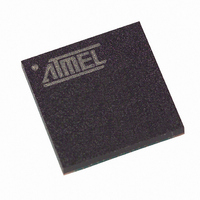
T89C51CC01CA-7CTIM Atmel, T89C51CC01CA-7CTIM Datasheet - Page 5

T89C51CC01CA-7CTIM
Manufacturer Part Number
T89C51CC01CA-7CTIM
Description
IC 8051 MCU FLASH 32K 64BGA
Manufacturer
Atmel
Series
AT89C CANr
Datasheets
1.T89C51CC01CA-7CTIM.pdf
(167 pages)
2.T89C51CC01CA-7CTIM.pdf
(12 pages)
3.T89C51CC01CA-7CTIM.pdf
(32 pages)
4.T89C51CC01CA-7CTIM.pdf
(29 pages)
Specifications of T89C51CC01CA-7CTIM
Core Processor
8051
Core Size
8-Bit
Speed
40MHz
Connectivity
CAN, UART/USART
Peripherals
POR, PWM, WDT
Number Of I /o
34
Program Memory Size
32KB (32K x 8)
Program Memory Type
FLASH
Eeprom Size
2K x 8
Ram Size
1.25K x 8
Voltage - Supply (vcc/vdd)
3 V ~ 5.5 V
Data Converters
A/D 8x10b
Oscillator Type
External
Operating Temperature
-40°C ~ 85°C
Package / Case
64-BGA
For Use With
AT89STK-06 - KIT DEMOBOARD 8051 MCU W/CAN
Lead Free Status / RoHS Status
Contains lead / RoHS non-compliant
Other names
T89C51CC01CA7CTIM
Available stocks
Company
Part Number
Manufacturer
Quantity
Price
- T89C51CC01CA-7CTIM PDF datasheet
- T89C51CC01CA-7CTIM PDF datasheet #2
- T89C51CC01CA-7CTIM PDF datasheet #3
- T89C51CC01CA-7CTIM PDF datasheet #4
- Current page: 5 of 167
- Download datasheet (2Mb)
Read-Modify-Write
Instructions
4129N–CAN–03/08
Figure 2. Port 0 Structure
Notes:
Figure 3. Port 2 Structure
Notes:
When Port 0 and Port 2 are used for an external memory cycle, an internal control signal
switches the output-driver input from the latch output to the internal address/data line.
Some instructions read the latch data rather than the pin data. The latch based instruc-
tions read the data, modify the data and then rewrite the latch. These are called "Read-
Modify-Write" instructions. Below is a complete list of these special instructions (see
Table ). When the destination operand is a Port or a Port bit, these instructions read the
latch rather than the pin:
READ
LATCH
INTERNAL
BUS
WRITE
TO
LATCH
READ
PIN
READ
LATCH
INTERNAL
BUS
WRITE
TO
LATCH
READ
PIN
1. Port 0 is precluded from use as general-purpose I/O Ports when used as
2. Port 0 internal strong pull-ups assist the logic-one output for memory bus cycles only.
1. Port 2 is precluded from use as general-purpose I/O Ports when as address/data bus
2. Port 2 internal strong pull-ups FET (P1 in FiGURE) assist the logic-one output for
address/data bus drivers.
Except for these bus cycles, the pull-up FET is off, Port 0 outputs are open-drain.
drivers.
memory bus cycle.
D
LATCH
P0.X
D
LATCH
P2.X
ADDRESS LOW/
DATA
Q
ADDRESS HIGH/ CONTROL
Q
CONTROL
1
0
1
0
VDD
VDD
(2)
INTERNAL
PULL-UP (2)
P0.x (1)
P2.x (1)
5
Related parts for T89C51CC01CA-7CTIM
Image
Part Number
Description
Manufacturer
Datasheet
Request
R

Part Number:
Description:
Enhanced 8-Bit Microcontroller
Manufacturer:
Atmel
Datasheet:

Part Number:
Description:
DEV KIT FOR AVR/AVR32
Manufacturer:
Atmel
Datasheet:

Part Number:
Description:
INTERVAL AND WIPE/WASH WIPER CONTROL IC WITH DELAY
Manufacturer:
ATMEL Corporation
Datasheet:

Part Number:
Description:
Low-Voltage Voice-Switched IC for Hands-Free Operation
Manufacturer:
ATMEL Corporation
Datasheet:

Part Number:
Description:
MONOLITHIC INTEGRATED FEATUREPHONE CIRCUIT
Manufacturer:
ATMEL Corporation
Datasheet:

Part Number:
Description:
AM-FM Receiver IC U4255BM-M
Manufacturer:
ATMEL Corporation
Datasheet:

Part Number:
Description:
Monolithic Integrated Feature Phone Circuit
Manufacturer:
ATMEL Corporation
Datasheet:

Part Number:
Description:
Multistandard Video-IF and Quasi Parallel Sound Processing
Manufacturer:
ATMEL Corporation
Datasheet:

Part Number:
Description:
High-performance EE PLD
Manufacturer:
ATMEL Corporation
Datasheet:

Part Number:
Description:
8-bit Flash Microcontroller
Manufacturer:
ATMEL Corporation
Datasheet:

Part Number:
Description:
2-Wire Serial EEPROM
Manufacturer:
ATMEL Corporation
Datasheet:


