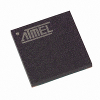
T89C51CC01CA-7CTIM Atmel, T89C51CC01CA-7CTIM Datasheet - Page 145

T89C51CC01CA-7CTIM
Manufacturer Part Number
T89C51CC01CA-7CTIM
Description
IC 8051 MCU FLASH 32K 64BGA
Manufacturer
Atmel
Series
AT89C CANr
Datasheets
1.T89C51CC01CA-7CTIM.pdf
(167 pages)
2.T89C51CC01CA-7CTIM.pdf
(12 pages)
3.T89C51CC01CA-7CTIM.pdf
(32 pages)
4.T89C51CC01CA-7CTIM.pdf
(29 pages)
Specifications of T89C51CC01CA-7CTIM
Core Processor
8051
Core Size
8-Bit
Speed
40MHz
Connectivity
CAN, UART/USART
Peripherals
POR, PWM, WDT
Number Of I /o
34
Program Memory Size
32KB (32K x 8)
Program Memory Type
FLASH
Eeprom Size
2K x 8
Ram Size
1.25K x 8
Voltage - Supply (vcc/vdd)
3 V ~ 5.5 V
Data Converters
A/D 8x10b
Oscillator Type
External
Operating Temperature
-40°C ~ 85°C
Package / Case
64-BGA
For Use With
AT89STK-06 - KIT DEMOBOARD 8051 MCU W/CAN
Lead Free Status / RoHS Status
Contains lead / RoHS non-compliant
Other names
T89C51CC01CA7CTIM
Available stocks
Company
Part Number
Manufacturer
Quantity
Price
- T89C51CC01CA-7CTIM PDF datasheet
- T89C51CC01CA-7CTIM PDF datasheet #2
- T89C51CC01CA-7CTIM PDF datasheet #3
- T89C51CC01CA-7CTIM PDF datasheet #4
- Current page: 145 of 167
- Download datasheet (2Mb)
4129N–CAN–03/08
Notes:
Figure 64. I
1. Operating I
2. Idle I
3. Power-down I
4. Capacitance loading on Ports 0 and 2 may cause spurious noise pulses to be super-
5. Typicals are based on a limited number of samples and are not guaranteed. The val-
6. Under steady state (non-transient) conditions, I
7. ICC_FLASH_WRITE operating current while a Flash block write is on going.
8. Flash Retention is guaranteed with the same formula for V
T
V
if a crystal oscillator used (see Figure 64.).
T
= V
V
and the POF flag must be set.
imposed on the V
capacitance discharging into the Port 0 and Port 2 pins when these pins make 1 to 0
transitions during bus operation. In the worst cases (capacitive loading 100pF), the
noise pulse on the ALE line may exceed 0.45V with maxi V
Trigger use is not necessary.
ues listed are at room temperature.
lows:
Maximum I
Maximum I
Port 0: 26 mA
Ports 1, 2 and 3: 15 mA
Maximum total I
If I
not guaranteed to sink current greater than the listed test conditions.
CLOCK
SIGNAL
CC
CLCH
IH
CHCL
CC
OL
SS
= V
; XTAL2 NC.; RST = V
Test Condition, Active Mode
(NC)
CC
exceeds the test condition, V
, T
(see Figure 65.).
= 5 ns, V
CC
CHCL
is measured with all output pins disconnected; XTAL1 driven with T
V
- 0.5V; XTAL2 N.C.; EA = RST = Port 0 = V
OL
OL
CC
CC
= 5 ns (see Figure 67.), V
CC
per port pin: 10 mA
per 8-bit port:
is measured with all output pins disconnected; XTAL1 driven with
IL
OL
RST
XTAL2
XTAL1
V
is measured with all output pins disconnected; EA = V
= V
SS
OL
for all output pins: 71 mA
s of ALE and Ports 1 and 3. The noise is due to external bus
SS
V
+ 0.5V, V
EA
CC
I
P0
CC
SS
V
(see Figure 66.). In addition, the WDT must be inactive
CC
V
IH
CC
= V
OL
may exceed the related specification. Pins are
CC
IL
= V
- 0.5V; XTAL2 N.C; Port 0 = V
SS
All other pins are disconnected.
+ 0.5V,
OL
must be externally limited as fol-
CC
. I
CC
CC
OL
would be slightly higher
Min down to 0.
peak 0.6V. A Schmitt
CC
CC
; EA = RST
, PORT 0 =
CLCH
145
,
Related parts for T89C51CC01CA-7CTIM
Image
Part Number
Description
Manufacturer
Datasheet
Request
R

Part Number:
Description:
Enhanced 8-Bit Microcontroller
Manufacturer:
Atmel
Datasheet:

Part Number:
Description:
DEV KIT FOR AVR/AVR32
Manufacturer:
Atmel
Datasheet:

Part Number:
Description:
INTERVAL AND WIPE/WASH WIPER CONTROL IC WITH DELAY
Manufacturer:
ATMEL Corporation
Datasheet:

Part Number:
Description:
Low-Voltage Voice-Switched IC for Hands-Free Operation
Manufacturer:
ATMEL Corporation
Datasheet:

Part Number:
Description:
MONOLITHIC INTEGRATED FEATUREPHONE CIRCUIT
Manufacturer:
ATMEL Corporation
Datasheet:

Part Number:
Description:
AM-FM Receiver IC U4255BM-M
Manufacturer:
ATMEL Corporation
Datasheet:

Part Number:
Description:
Monolithic Integrated Feature Phone Circuit
Manufacturer:
ATMEL Corporation
Datasheet:

Part Number:
Description:
Multistandard Video-IF and Quasi Parallel Sound Processing
Manufacturer:
ATMEL Corporation
Datasheet:

Part Number:
Description:
High-performance EE PLD
Manufacturer:
ATMEL Corporation
Datasheet:

Part Number:
Description:
8-bit Flash Microcontroller
Manufacturer:
ATMEL Corporation
Datasheet:

Part Number:
Description:
2-Wire Serial EEPROM
Manufacturer:
ATMEL Corporation
Datasheet:


