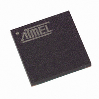
T89C51CC01CA-7CTIM Atmel, T89C51CC01CA-7CTIM Datasheet - Page 24

T89C51CC01CA-7CTIM
Manufacturer Part Number
T89C51CC01CA-7CTIM
Description
IC 8051 MCU FLASH 32K 64BGA
Manufacturer
Atmel
Series
AT89C CANr
Datasheets
1.T89C51CC01CA-7CTIM.pdf
(167 pages)
2.T89C51CC01CA-7CTIM.pdf
(12 pages)
3.T89C51CC01CA-7CTIM.pdf
(32 pages)
4.T89C51CC01CA-7CTIM.pdf
(29 pages)
Specifications of T89C51CC01CA-7CTIM
Core Processor
8051
Core Size
8-Bit
Speed
40MHz
Connectivity
CAN, UART/USART
Peripherals
POR, PWM, WDT
Number Of I /o
34
Program Memory Size
32KB (32K x 8)
Program Memory Type
FLASH
Eeprom Size
2K x 8
Ram Size
1.25K x 8
Voltage - Supply (vcc/vdd)
3 V ~ 5.5 V
Data Converters
A/D 8x10b
Oscillator Type
External
Operating Temperature
-40°C ~ 85°C
Package / Case
64-BGA
For Use With
AT89STK-06 - KIT DEMOBOARD 8051 MCU W/CAN
Lead Free Status / RoHS Status
Contains lead / RoHS non-compliant
Other names
T89C51CC01CA7CTIM
Available stocks
Company
Part Number
Manufacturer
Quantity
Price
Internal Space
Lower 128 Bytes RAM
Upper 128 Bytes RAM
Expanded RAM
24
A/T89C51CC01
The lower 128 Bytes of RAM (see Figure 11) are accessible from address 00h to 7Fh
using direct or indirect addressing modes. The lowest 32 Bytes are grouped into 4
banks of 8 registers (R0 to R7). Two bits RS0 and RS1 in PSW register (see Figure 18)
select which bank is in use according to Table 16. This allows more efficient use of code
space, since register instructions are shorter than instructions that use direct address-
ing, and can be used for context switching in interrupt service routines.
Table 16. Register Bank Selection
The next 16 Bytes above the register banks form a block of bit-addressable memory
space. The C51 instruction set includes a wide selection of single-bit instructions, and
the 128 bits in this area can be directly addressed by these instructions. The bit
addresses in this area are 00h to 7Fh.
Figure 12. Lower 128 Bytes Internal RAM Organization
The upper 128 Bytes of RAM are accessible from address 80h to FFh using only indirect
addressing mode.
The on-chip 1024 Bytes of expanded RAM (XRAM) are accessible from address 0000h
to 03FFh using indirect addressing mode through MOVX instructions. In this address
range, the bit EXTRAM in AUXR register is used to select the XRAM (default) or the
XRAM. As shown in Figure 11 when EXTRAM = 0, the XRAM is selected and when
EXTRAM = 1, the XRAM is selected.
The size of XRAM can be configured by XRS1-0 bit in AUXR register (default size is
1024 Bytes).
Note:
RS1
Lower 128 Bytes RAM, Upper 128 Bytes RAM, and expanded RAM are made of volatile
memory cells. This means that the RAM content is indeterminate after power-up and
must then be initialized properly.
0
0
1
1
RS0
0
1
0
1
30h
20h
18h
10h
08h
00h
Description
Register bank 0 from 00h to 07h
Register bank 0 from 08h to 0Fh
Register bank 0 from 10h to 17h
Register bank 0 from 18h to 1Fh
7Fh
2Fh
1Fh
0Fh
17h
07h
Bit-Addressable Space
(Bit Addresses 0-7Fh)
4 Banks of
8 Registers
R0-R7
4129N–CAN–03/08


