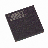
T89C51CC01CA-7CTIM Atmel, T89C51CC01CA-7CTIM Datasheet - Page 131

T89C51CC01CA-7CTIM
Manufacturer Part Number
T89C51CC01CA-7CTIM
Description
IC 8051 MCU FLASH 32K 64BGA
Manufacturer
Atmel
Series
AT89C CANr
Datasheets
1.T89C51CC01CA-7CTIM.pdf
(167 pages)
2.T89C51CC01CA-7CTIM.pdf
(12 pages)
3.T89C51CC01CA-7CTIM.pdf
(32 pages)
4.T89C51CC01CA-7CTIM.pdf
(29 pages)
Specifications of T89C51CC01CA-7CTIM
Core Processor
8051
Core Size
8-Bit
Speed
40MHz
Connectivity
CAN, UART/USART
Peripherals
POR, PWM, WDT
Number Of I /o
34
Program Memory Size
32KB (32K x 8)
Program Memory Type
FLASH
Eeprom Size
2K x 8
Ram Size
1.25K x 8
Voltage - Supply (vcc/vdd)
3 V ~ 5.5 V
Data Converters
A/D 8x10b
Oscillator Type
External
Operating Temperature
-40°C ~ 85°C
Package / Case
64-BGA
For Use With
AT89STK-06 - KIT DEMOBOARD 8051 MCU W/CAN
Lead Free Status / RoHS Status
Contains lead / RoHS non-compliant
Other names
T89C51CC01CA7CTIM
Available stocks
Company
Part Number
Manufacturer
Quantity
Price
- T89C51CC01CA-7CTIM PDF datasheet
- T89C51CC01CA-7CTIM PDF datasheet #2
- T89C51CC01CA-7CTIM PDF datasheet #3
- T89C51CC01CA-7CTIM PDF datasheet #4
- Current page: 131 of 167
- Download datasheet (2Mb)
ADC Converter
Operation
Voltage Conversion
Clock Selection
4129N–CAN–03/08
A start of single A/D conversion is triggered by setting bit ADSST (ADCON.3).
After completion of the A/D conversion, the ADSST bit is cleared by hardware.
The end-of-conversion flag ADEOC (ADCON.4) is set when the value of conversion is
available in ADDH and ADDL, it must be cleared by software. If the bit EADC (IEN1.1) is
set, an interrupt occur when flag ADEOC is set (see Figure 62). Clear this flag for re-
arming the interrupt.
The bits SCH0 to SCH2 in ADCON register are used for the analog input channel
selection.
Note:
Table 107. Selected Analog input
When the ADCIN is equals to VAREF the ADC converts the signal to 3FFh (full scale). If
the input voltage equals VAGND, the ADC converts it to 000h. Input voltage between
VAREF and VAGND are a straight-line linear conversion. All other voltages will result in
3FFh if greater than VAREF and 000h if less than VAGND.
Note:
The ADC clock is the same as CPU.
The maximum clock frequency is defined in the DC parmeters for A/D converter. A pres-
caler is featured (ADCCLK) to generate the ADC clock from the oscillator frequency.
if PRS > 0 then f
if PRS = 0 then f
1. Always leave Tsetup time before starting a conversion unless ADEN is permanently
ADCIN should not exceed VAREF absolute maximum range (see “Absolute Maximum
Ratings” on page 144)
SCH2
(1)
0
0
0
0
1
1
1
1
high. In this case one should wait Tsetup only before the first conversion.
ADC
ADC
= F
= F
periph
periph
/ 2 x PRS
/ 64
SCH1
0
0
1
1
0
0
1
1
SCH0
0
1
0
1
0
1
0
1
Selected Analog input
AN0
AN1
AN2
AN3
AN4
AN5
AN6
AN7
131
Related parts for T89C51CC01CA-7CTIM
Image
Part Number
Description
Manufacturer
Datasheet
Request
R

Part Number:
Description:
Enhanced 8-Bit Microcontroller
Manufacturer:
Atmel
Datasheet:

Part Number:
Description:
DEV KIT FOR AVR/AVR32
Manufacturer:
Atmel
Datasheet:

Part Number:
Description:
INTERVAL AND WIPE/WASH WIPER CONTROL IC WITH DELAY
Manufacturer:
ATMEL Corporation
Datasheet:

Part Number:
Description:
Low-Voltage Voice-Switched IC for Hands-Free Operation
Manufacturer:
ATMEL Corporation
Datasheet:

Part Number:
Description:
MONOLITHIC INTEGRATED FEATUREPHONE CIRCUIT
Manufacturer:
ATMEL Corporation
Datasheet:

Part Number:
Description:
AM-FM Receiver IC U4255BM-M
Manufacturer:
ATMEL Corporation
Datasheet:

Part Number:
Description:
Monolithic Integrated Feature Phone Circuit
Manufacturer:
ATMEL Corporation
Datasheet:

Part Number:
Description:
Multistandard Video-IF and Quasi Parallel Sound Processing
Manufacturer:
ATMEL Corporation
Datasheet:

Part Number:
Description:
High-performance EE PLD
Manufacturer:
ATMEL Corporation
Datasheet:

Part Number:
Description:
8-bit Flash Microcontroller
Manufacturer:
ATMEL Corporation
Datasheet:

Part Number:
Description:
2-Wire Serial EEPROM
Manufacturer:
ATMEL Corporation
Datasheet:


