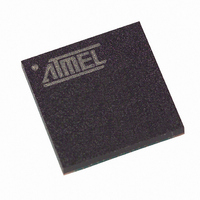
T89C51CC01CA-7CTIM Atmel, T89C51CC01CA-7CTIM Datasheet - Page 4

T89C51CC01CA-7CTIM
Manufacturer Part Number
T89C51CC01CA-7CTIM
Description
IC 8051 MCU FLASH 32K 64BGA
Manufacturer
Atmel
Series
AT89C CANr
Datasheets
1.T89C51CC01CA-7CTIM.pdf
(167 pages)
2.T89C51CC01CA-7CTIM.pdf
(12 pages)
3.T89C51CC01CA-7CTIM.pdf
(32 pages)
4.T89C51CC01CA-7CTIM.pdf
(29 pages)
Specifications of T89C51CC01CA-7CTIM
Core Processor
8051
Core Size
8-Bit
Speed
40MHz
Connectivity
CAN, UART/USART
Peripherals
POR, PWM, WDT
Number Of I /o
34
Program Memory Size
32KB (32K x 8)
Program Memory Type
FLASH
Eeprom Size
2K x 8
Ram Size
1.25K x 8
Voltage - Supply (vcc/vdd)
3 V ~ 5.5 V
Data Converters
A/D 8x10b
Oscillator Type
External
Operating Temperature
-40°C ~ 85°C
Package / Case
64-BGA
For Use With
AT89STK-06 - KIT DEMOBOARD 8051 MCU W/CAN
Lead Free Status / RoHS Status
Contains lead / RoHS non-compliant
Other names
T89C51CC01CA7CTIM
Available stocks
Company
Part Number
Manufacturer
Quantity
Price
I/O Configurations
Port 1, Port 3 and Port 4
Port 0 and Port 2
4
A/T89C51CC01
Each Port SFR operates via type-D latches, as illustrated in Figure 1 for Ports 3 and 4. A
CPU "write to latch" signal initiates transfer of internal bus data into the type-D latch. A
CPU "read latch" signal transfers the latched Q output onto the internal bus. Similarly, a
"read pin" signal transfers the logical level of the Port pin. Some Port data instructions
activate the "read latch" signal while others activate the "read pin" signal. Latch instruc-
tions are referred to as Read-Modify-Write instructions. Each I/O line may be
independently programmed as input or output.
Figure 1 shows the structure of Ports 1 and 3, which have internal pull-ups. An external
source can pull the pin low. Each Port pin can be configured either for general-purpose
I/O or for its alternate input output function.
To use a pin for general-purpose output, set or clear the corresponding bit in the Px reg-
ister (x = 1,3 or 4). To use a pin for general-purpose input, set the bit in the Px register.
This turns off the output FET drive.
To configure a pin for its alternate function, set the bit in the Px register. When the latch
is set, the "alternate output function" signal controls the output level (see Figure 1). The
operation of Ports 1, 3 and 4 is discussed further in the "quasi-Bidirectional Port Opera-
tion" section.
Figure 1. Port 1, Port 3 and Port 4 Structure
Note:
Ports 0 and 2 are used for general-purpose I/O or as the external address/data bus. Port
0, shown in Figure 3, differs from the other Ports in not having internal pull-ups. Figure 3
shows the structure of Port 2. An external source can pull a Port 2 pin low.
To use a pin for general-purpose output, set or clear the corresponding bit in the Px reg-
ister (x = 0 or 2). To use a pin for general-purpose input, set the bit in the Px register to
turn off the output driver FET.
READ
LATCH
INTERNAL
BUS
WRITE
TO
LATCH
The internal pull-up can be disabled on P1 when analog function is selected.
READ
PIN
D
CL
LATCH
P1.X
P3.X
P4.X
Q
ALTERNATE
OUTPUT
FUNCTION
ALTERNATE
INPUT
FUNCTION
VCC
INTERNAL
PULL-UP (1)
4129N–CAN–03/08
P1.x
P3.x
P4.x


