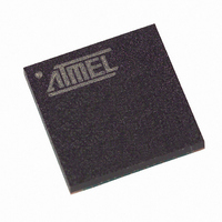
T89C51CC01CA-7CTIM Atmel, T89C51CC01CA-7CTIM Datasheet - Page 144

T89C51CC01CA-7CTIM
Manufacturer Part Number
T89C51CC01CA-7CTIM
Description
IC 8051 MCU FLASH 32K 64BGA
Manufacturer
Atmel
Series
AT89C CANr
Datasheets
1.T89C51CC01CA-7CTIM.pdf
(167 pages)
2.T89C51CC01CA-7CTIM.pdf
(12 pages)
3.T89C51CC01CA-7CTIM.pdf
(32 pages)
4.T89C51CC01CA-7CTIM.pdf
(29 pages)
Specifications of T89C51CC01CA-7CTIM
Core Processor
8051
Core Size
8-Bit
Speed
40MHz
Connectivity
CAN, UART/USART
Peripherals
POR, PWM, WDT
Number Of I /o
34
Program Memory Size
32KB (32K x 8)
Program Memory Type
FLASH
Eeprom Size
2K x 8
Ram Size
1.25K x 8
Voltage - Supply (vcc/vdd)
3 V ~ 5.5 V
Data Converters
A/D 8x10b
Oscillator Type
External
Operating Temperature
-40°C ~ 85°C
Package / Case
64-BGA
For Use With
AT89STK-06 - KIT DEMOBOARD 8051 MCU W/CAN
Lead Free Status / RoHS Status
Contains lead / RoHS non-compliant
Other names
T89C51CC01CA7CTIM
Available stocks
Company
Part Number
Manufacturer
Quantity
Price
Electrical Characteristics
Absolute Maximum Ratings
DC Parameters for Standard Voltage
T
Table 121. DC Parameters in Standard Voltage
144
Ambiant Temperature Under Bias:
I = industrial ....................................................... -40°C to 85°C
Storage Temperature .................................... -65°C to + 150°C
Voltage on V
Voltage on Any Pin from V
Power Dissipation .............................................................. 1 W
A
Symbol
= -40°C to +85°C; V
V
V
R
V
V
V
V
C
V
IH1
I
I
I
OH1
I
I
CC
OL1
RST
PD
TL
OL
OH
IL
LI
IH
IO
IL
(8)
A/T89C51CC01
Parameter
Input Low Voltage
Input High Voltage except XTAL1, RST
Input High Voltage, XTAL1, RST
Output Low Voltage, ports 1, 2, 3 and 4
Output Low Voltage, port 0, ALE, PSEN
Output High Voltage, ports 1, 2, 3, 4 and 5
Output High Voltage, port 0, ALE, PSEN
RST Pulldown Resistor
Logical 0 Input Current ports 1, 2, 3 and 4
Input Leakage Current
Logical 1 to 0 Transition Current, ports 1, 2, 3
and 4
Capacitance of I/O Buffer
Power-down Current
Power Supply Current
CC
from V
SS
......................................-0.5V to + 6V
SS
SS
= 0V; V
.................... -0.5V to V
CC
= 3V to 5.5V; F = 0 to 40 MHz
(6)
(6)
CC
+ 0.2 V
0.2 V
ICC_FLASH_WRITE
V
V
V
V
V
V
0.7 V
CC
CC
CC
CC
CC
CC
Min
-0.5
CC
15
- 0.3
- 0.7
- 1.5
- 0.3
- 0.7
- 1.5
CC
+ 0.9
I
*NOTICE:
I
CCIDLE
CCOP
= 0.7 Freq (MHz) + 3 mA
= 0.6 Freq (MHz) + 2 mA
(7)
Typ
160
40
=0.4 Freq (MHz) + 20 ma
Stresses at or above those listed under “Absolute Max-
imum Ratings” may cause permanent damage to the
device. This is a stress rating only and functional oper-
ation of the device at these or any other conditions
above those indicated in the operational sections of
this specification is not implied. Exposure to absolute
maximum rating conditions may affect device reliability.
The power dissipation is based on the maximum allow-
able die temperature and the thermal resistance of the
package.
(5)
0.2Vcc - 0.1
V
V
CC
CC
Max
0.45
0.45
-650
200
±10
400
0.3
1.0
0.3
1.0
-50
10
+ 0.5
+ 0.5
Unit
kΩ
µA
µA
µA
µA
pF
V
V
V
V
V
V
V
V
V
V
V
V
V
V
V
I
I
I
I
I
I
I
I
I
I
I
I
Vin = 0.45V
0.45V < Vin < V
Vin = 2.0V
Fc = 1 MHz
T
3V < V
3V < V
OL
OL
OL
OL
OL
OL
OH
OH
OH
OH
OH
OH
A
= 25°C
= 100 µA
= 1.6 mA
= 3.5 mA
= 200 µA
= 3.2 mA
= 7.0 mA
= -10 µA
= -30 µA
= -60 µA
= -200 µA
= -3.2 mA
= -7.0 mA
Test Conditions
CC
CC
< 5.5V
< 5.5V
4129N–CAN–03/08
(4)
(4)
(4)
(4)
(4)
(4)
CC
(3)
(1)(2)


