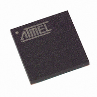
T89C51CC01CA-7CTIM Atmel, T89C51CC01CA-7CTIM Datasheet - Page 34

T89C51CC01CA-7CTIM
Manufacturer Part Number
T89C51CC01CA-7CTIM
Description
IC 8051 MCU FLASH 32K 64BGA
Manufacturer
Atmel
Series
AT89C CANr
Datasheets
1.T89C51CC01CA-7CTIM.pdf
(167 pages)
2.T89C51CC01CA-7CTIM.pdf
(12 pages)
3.T89C51CC01CA-7CTIM.pdf
(32 pages)
4.T89C51CC01CA-7CTIM.pdf
(29 pages)
Specifications of T89C51CC01CA-7CTIM
Core Processor
8051
Core Size
8-Bit
Speed
40MHz
Connectivity
CAN, UART/USART
Peripherals
POR, PWM, WDT
Number Of I /o
34
Program Memory Size
32KB (32K x 8)
Program Memory Type
FLASH
Eeprom Size
2K x 8
Ram Size
1.25K x 8
Voltage - Supply (vcc/vdd)
3 V ~ 5.5 V
Data Converters
A/D 8x10b
Oscillator Type
External
Operating Temperature
-40°C ~ 85°C
Package / Case
64-BGA
For Use With
AT89STK-06 - KIT DEMOBOARD 8051 MCU W/CAN
Lead Free Status / RoHS Status
Contains lead / RoHS non-compliant
Other names
T89C51CC01CA7CTIM
Available stocks
Company
Part Number
Manufacturer
Quantity
Price
- T89C51CC01CA-7CTIM PDF datasheet
- T89C51CC01CA-7CTIM PDF datasheet #2
- T89C51CC01CA-7CTIM PDF datasheet #3
- T89C51CC01CA-7CTIM PDF datasheet #4
- Current page: 34 of 167
- Download datasheet (2Mb)
17.22 External Code Memory Access
Memory Interface
External Bus Cycles
34
A/T89C51CC01
The external memory interface comprises the external bus (port 0 and port 2) as well as
the bus control signals (PSEN#, and ALE).
Figure 18 shows the structure of the external address bus. P0 carries address A7:0
while P2 carries address A15:8. Data D7:0 is multiplexed with A7:0 on P0. Table 18
describes the external memory interface signals.
Figure 18. External Code Memory Interface Structure
Table 23. External Code Memory Interface Signals
This section describes the bus cycles the T89C51CC01 executes to fetch code (see
Figure 19) in the external program/code memory.
External memory cycle takes 6 CPU clock periods. This is equivalent to 12 oscillator
clock period in standard mode or 6 oscillator clock periods in X2 mode. For further infor-
mation on X2 mode see section “Clock “.
For simplicity, the accompanying figure depicts the bus cycle waveforms in idealized
form and do not provide precise timing information.
For bus cycling parameters refer to the ‘AC-DC parameters’ section.
Signal
PSEN#
Name
AD7:0
A15:8
ALE
Type
I/O
O
O
O
Description
Address Lines
Upper address lines for the external bus.
Address/Data Lines
Multiplexed lower address lines and data for the external memory.
Address Latch Enable
ALE signals indicates that valid address information are available on lines
AD7:0.
Program Store Enable Output
This signal is active low during external code fetch or external code read
(MOVC instruction).
T89C51CC01
PSEN#
ALE
P2
P0
AD7:0
A15:8
Latch
A7:0
A15:8
A7:0
D7:0
OE
EPROM
Flash
4129N–CAN–03/08
Alternate
Function
P2.7:0
P0.7:0
-
-
Related parts for T89C51CC01CA-7CTIM
Image
Part Number
Description
Manufacturer
Datasheet
Request
R

Part Number:
Description:
Enhanced 8-Bit Microcontroller
Manufacturer:
Atmel
Datasheet:

Part Number:
Description:
DEV KIT FOR AVR/AVR32
Manufacturer:
Atmel
Datasheet:

Part Number:
Description:
INTERVAL AND WIPE/WASH WIPER CONTROL IC WITH DELAY
Manufacturer:
ATMEL Corporation
Datasheet:

Part Number:
Description:
Low-Voltage Voice-Switched IC for Hands-Free Operation
Manufacturer:
ATMEL Corporation
Datasheet:

Part Number:
Description:
MONOLITHIC INTEGRATED FEATUREPHONE CIRCUIT
Manufacturer:
ATMEL Corporation
Datasheet:

Part Number:
Description:
AM-FM Receiver IC U4255BM-M
Manufacturer:
ATMEL Corporation
Datasheet:

Part Number:
Description:
Monolithic Integrated Feature Phone Circuit
Manufacturer:
ATMEL Corporation
Datasheet:

Part Number:
Description:
Multistandard Video-IF and Quasi Parallel Sound Processing
Manufacturer:
ATMEL Corporation
Datasheet:

Part Number:
Description:
High-performance EE PLD
Manufacturer:
ATMEL Corporation
Datasheet:

Part Number:
Description:
8-bit Flash Microcontroller
Manufacturer:
ATMEL Corporation
Datasheet:

Part Number:
Description:
2-Wire Serial EEPROM
Manufacturer:
ATMEL Corporation
Datasheet:


