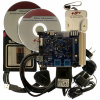
C8051F930DK Silicon Laboratories Inc, C8051F930DK Datasheet - Page 244

C8051F930DK
Manufacturer Part Number
C8051F930DK
Description
KIT DEV C8051F920,F921,F930,F931
Manufacturer
Silicon Laboratories Inc
Type
MCUr
Specifications of C8051F930DK
Contents
Target Board, Power Adapter, USB Debug Adapter, Cables, Batteries, and Software
Processor To Be Evaluated
C8051F930
Processor Series
C8051F9xx
Data Bus Width
8 bit
Interface Type
I2C, UART, SPI
Maximum Operating Temperature
+ 85 C
Minimum Operating Temperature
- 40 C
Operating Supply Voltage
0.9 V to 3.6 V
Lead Free Status / RoHS Status
Lead free / RoHS Compliant
For Use With/related Products
C8051F920, F921, F930, F931
Lead Free Status / Rohs Status
Lead free / RoHS Compliant
Other names
336-1473
Available stocks
Company
Part Number
Manufacturer
Quantity
Price
Company:
Part Number:
C8051F930DK
Manufacturer:
Silicon Labs
Quantity:
135
- Current page: 244 of 324
- Download datasheet (3Mb)
C8051F93x-C8051F92x
22.4.3. Hardware Slave Address Recognition
The SMBus hardware has the capability to automatically recognize incoming slave addresses and send an
ACK without software intervention. Automatic slave address recognition is enabled by setting the EHACK
bit in register SMB0ADM to 1. This will enable both automatic slave address recognition and automatic
hardware ACK generation for received bytes (as a master or slave). More detail on automatic hardware
ACK generation can be found in Section 22.4.2.2.
The registers used to define which address(es) are recognized by the hardware are the SMBus Slave
Address register (SFR Definition 22.3) and the SMBus Slave Address Mask register (SFR Definition 22.4).
A single address or range of addresses (including the General Call Address 0x00) can be specified using
these two registers. The most-significant seven bits of the two registers are used to define which
addresses will be ACKed. A 1 in bit positions of the slave address mask SLVM[6:0] enable a comparison
between the received slave address and the hardware’s slave address SLV[6:0] for those bits. A 0 in a bit
of the slave address mask means that bit will be treated as a “don’t care” for comparison purposes. In this
case, either a 1 or a 0 value are acceptable on the incoming slave address. Additionally, if the GC bit in
register SMB0ADR is set to 1, hardware will recognize the General Call Address (0x00). Table 22.4 shows
some example parameter settings and the slave addresses that will be recognized by hardware under
those conditions. Refer to the C8051F930 errata when using hardware ACK generation on
C8051F930/31/20/21 devices.
244
Hardware Slave Address
SLV[6:0]
0x34
0x34
0x34
0x34
0x70
Table 22.4. Hardware Address Recognition Examples (EHACK = 1)
Slave Address Mask
SLVM[6:0]
0x7F
0x7F
0x7E
0x7E
0x73
Rev. 1.1
GC bit
0
1
0
1
0
Slave Addresses Recognized by
Hardware
0x34
0x34, 0x00 (General Call)
0x34, 0x35
0x34, 0x35, 0x00 (General Call)
0x70, 0x74, 0x78, 0x7C
Related parts for C8051F930DK
Image
Part Number
Description
Manufacturer
Datasheet
Request
R
Part Number:
Description:
SMD/C°/SINGLE-ENDED OUTPUT SILICON OSCILLATOR
Manufacturer:
Silicon Laboratories Inc
Part Number:
Description:
Manufacturer:
Silicon Laboratories Inc
Datasheet:
Part Number:
Description:
N/A N/A/SI4010 AES KEYFOB DEMO WITH LCD RX
Manufacturer:
Silicon Laboratories Inc
Datasheet:
Part Number:
Description:
N/A N/A/SI4010 SIMPLIFIED KEY FOB DEMO WITH LED RX
Manufacturer:
Silicon Laboratories Inc
Datasheet:
Part Number:
Description:
N/A/-40 TO 85 OC/EZLINK MODULE; F930/4432 HIGH BAND (REV E/B1)
Manufacturer:
Silicon Laboratories Inc
Part Number:
Description:
EZLink Module; F930/4432 Low Band (rev e/B1)
Manufacturer:
Silicon Laboratories Inc
Part Number:
Description:
I°/4460 10 DBM RADIO TEST CARD 434 MHZ
Manufacturer:
Silicon Laboratories Inc
Part Number:
Description:
I°/4461 14 DBM RADIO TEST CARD 868 MHZ
Manufacturer:
Silicon Laboratories Inc
Part Number:
Description:
I°/4463 20 DBM RFSWITCH RADIO TEST CARD 460 MHZ
Manufacturer:
Silicon Laboratories Inc
Part Number:
Description:
I°/4463 20 DBM RADIO TEST CARD 868 MHZ
Manufacturer:
Silicon Laboratories Inc
Part Number:
Description:
I°/4463 27 DBM RADIO TEST CARD 868 MHZ
Manufacturer:
Silicon Laboratories Inc
Part Number:
Description:
I°/4463 SKYWORKS 30 DBM RADIO TEST CARD 915 MHZ
Manufacturer:
Silicon Laboratories Inc
Part Number:
Description:
N/A N/A/-40 TO 85 OC/4463 RFMD 30 DBM RADIO TEST CARD 915 MHZ
Manufacturer:
Silicon Laboratories Inc
Part Number:
Description:
I°/4463 20 DBM RADIO TEST CARD 169 MHZ
Manufacturer:
Silicon Laboratories Inc


