HW-SPAR3E-SK-UK-G Xilinx Inc, HW-SPAR3E-SK-UK-G Datasheet - Page 77
HW-SPAR3E-SK-UK-G
Manufacturer Part Number
HW-SPAR3E-SK-UK-G
Description
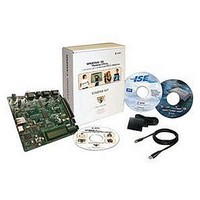
KIT STARTER SPARTAN-3E
Manufacturer
Xilinx Inc
Specifications of HW-SPAR3E-SK-UK-G
Tool / Board Applications
General Purpose MCU, MPU, DSP, DSC
Development Tool Type
Hardware / Software - Starter Kit
Mcu Supported Families
Spartan-3E
Lead Free Status / RoHS Status
Lead free / RoHS Compliant
Other names
HW-SPAR3E-SK-US-UK-G
HW-SPAR3E-SK-US-UK-G
HW-SPAR3E-SK-US-UK-G
Available stocks
Company
Part Number
Manufacturer
Quantity
Price


Programmable Pre-Amplifier
Spartan-3E FPGA Starter Kit Board User Guide
UG230 (v1.2) January 20, 2011
Interface
Programmable Gain
R
Finally, the ADC presents a 14-bit, two’s complement digital output. A 14-bit, two’s
complement number represents values between -2
scaled by 8192, or 2
See
pre-amplifier.
The reference design files provide more information on converting the voltage applied on
VINA or VINB to a digital representation (see
The LTC6912-1 provides two independent inverting amplifiers with programmable gain.
The purpose of the amplifier is to scale the incoming voltage on VINA or VINB so that it
maximizes the conversion range of the DAC, namely 1.65 ± 1.25V.
Table 10-1
SPI_MISO, and SPI_SCK signals are shared with other devices on the SPI bus. The
AMP_CS signal is the active-Low slave select input to the amplifier.
Table 10-1: AMP Interface Signals
Each analog channel has an associated programmable gain amplifier (see
Analog signals presented on the VINA or VINB inputs on header J7 are amplified relative
to 1.65V. The 1.65V reference is generated using a voltage divider of the 3.3V voltage
supply.
The gain of each amplifier is programmable from -1 to -100, as shown in
Table 10-2: Programmable Gain Settings for Pre-Amplifier
SPI_MOSI
AMP_CS
SPI_SCK
AMP_SHDN
AMP_DOUT
“Programmable Pre-Amplifier”
Gain
Signal
-1
-2
0
lists the interface signals between the FPGA and the amplifier. The SPI_MOSI,
FPGA Pin
A3
B3
13
0
0
0
U16
E18
N7
T4
P7
.
www.xilinx.com
FPGAAMP
FPGAAMP
FPGAAMP
FPGAAMP
FPGAAD
A2
B2
Direction
0
0
0
to control the GAIN settings on the programmable
A1
B1
0
0
1
Serial data: Master Output, Slave Input.
Presents 8-bit programmable gain settings, as
defined in
set when signal returns High.
Clock
settings. Can be ignored in most applications.
Active-Low chip-select. The amplifier gain is
Active-High shutdown, reset
Serial data. Echoes previous amplifier gain
“Related Resources,” page
13
and 2
Table
A0
B0
0
1
0
13
Programmable Pre-Amplifier
-1. Therefore, the quantity is
Description
10-2.
Minimum
Input Voltage Range
1.025
0.4
Table
81).
Figure
Maximum
10-2.
10-2).
2.275
2.9
77
Related parts for HW-SPAR3E-SK-UK-G
Image
Part Number
Description
Manufacturer
Datasheet
Request
R

Part Number:
Description:
KIT STARTER SPARTAN-3E
Manufacturer:
Xilinx Inc
Datasheet:
Part Number:
Description:
KIT STARTER SPARTAN-3E
Manufacturer:
Xilinx Inc
Datasheet:
Part Number:
Description:
KIT DEV SPARTAN3E DISPLAY
Manufacturer:
Xilinx Inc
Part Number:
Description:
KIT DEV SPARTAN3E DISPLAY
Manufacturer:
Xilinx Inc
Datasheet:

Part Number:
Description:
IC CPLD .8K 36MCELL 44-VQFP
Manufacturer:
Xilinx Inc
Datasheet:

Part Number:
Description:
IC CPLD 72MCRCELL 10NS 44VQFP
Manufacturer:
Xilinx Inc
Datasheet:

Part Number:
Description:
IC CPLD 1.6K 72MCELL 64-VQFP
Manufacturer:
Xilinx Inc
Datasheet:

Part Number:
Description:
IC CR-II CPLD 64MCELL 44-VQFP
Manufacturer:
Xilinx Inc
Datasheet:

Part Number:
Description:
IC CPLD 1.6K 72MCELL 100-TQFP
Manufacturer:
Xilinx Inc
Datasheet:

Part Number:
Description:
IC CR-II CPLD 64MCELL 56-BGA
Manufacturer:
Xilinx Inc
Datasheet:

Part Number:
Description:
IC CPLD 72MCRCELL 7.5NS 44VQFP
Manufacturer:
Xilinx Inc
Datasheet:
Part Number:
Description:
IC CR-II CPLD 64MCELL 100-VQFP
Manufacturer:
Xilinx Inc
Datasheet: