HW-SPAR3E-SK-UK-G Xilinx Inc, HW-SPAR3E-SK-UK-G Datasheet - Page 101
HW-SPAR3E-SK-UK-G
Manufacturer Part Number
HW-SPAR3E-SK-UK-G
Description
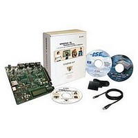
KIT STARTER SPARTAN-3E
Manufacturer
Xilinx Inc
Specifications of HW-SPAR3E-SK-UK-G
Tool / Board Applications
General Purpose MCU, MPU, DSP, DSC
Development Tool Type
Hardware / Software - Starter Kit
Mcu Supported Families
Spartan-3E
Lead Free Status / RoHS Status
Lead free / RoHS Compliant
Other names
HW-SPAR3E-SK-US-UK-G
HW-SPAR3E-SK-US-UK-G
HW-SPAR3E-SK-US-UK-G
Available stocks
Company
Part Number
Manufacturer
Quantity
Price


Spartan-3E FPGA Starter Kit Board User Guide
UG230 (v1.2) January 20, 2011
Other SPI Flash Control Signals
Variant Select Pins, VS[2:0]
Jumper Block J11
Programming Header J12
Multi-Package Layout
R
Table 12-3: Disable Other Devices on SPI Bus
The M25P16 SPI Flash has two additional control inputs. The active-Low write protect
input (W) and the active-Low bus hold input (HLD) are unused and pulled High via an
external pull-up resistor.
When in SPI configuration mode, the FPGA samples the value on three pins, labeled
VS[2:0], to determine which SPI read command to issue to the SPI Flash. For the M25P16
Flash, VS[2:0]=<1:1:1> issues the correct command sequence. The VS[2:0] pins are pulled
High externally via pull-up resistors to 3.3V. The VS[2:0] pins are also parallel NOR Flash
address lines A[19:17] in the FPGA’s BPI configuration mode and these signals also
connect to the StrataFlash parallel Flash PROM. After SPI configuration, the VS[2:0] pins
become user-programmable I/O pins, allowing full access to the StrataFlash PROM,
despite that the FPGA configured from SPI Flash.
In SPI configuration mode, the FPGA selects the attached SPI Flash by asserting the CSO_B
pin Low. On the Spartan-3E Starter Kit board, the CSO_B pin drives into the jumper J11
block. This jumper block provides the option to move the on-board SPI Flash to a different
select line (SPI_ALT_CS_JP11). This way, a different SPI Flash device can be tested by
changing the JP11 jumper settings and connecting the alternate SPI Flash on Header JP12.
By default, both jumpers are inserted on jumper block header J11.
As shown in
to program the on-board SPI Flash.
STMicroelectronics was rather clever when they defined the package layout for the
M25Pxx SPI serial Flash family. The Spartan-3E Starter Kit board supports all three of the
package types used for the 16 Mbit device, as shown in
ships with the 8-lead, 8x6 mm MLP package. The multi-package layout also supports the 8-
pin SOIC package and the 16-pin SOIC package. Pin 1 for the 8-pin SOIC and MLP
packages is located in the top-left corner. However, pin 1 for the 16-pin SOIC package is
located in the top-right corner, because the package is rotated 90
package also have four pins on each side that do not connect on the board. These pins must
DAC_CS
AMP_CS
AD_CONV
SF_CE0
FPGA_INIT_B
Signal
Figure 12-15, page
Digital-to-Analog Converter (DAC)
Programmable Pre-Amplifier
Analog-to-Digital Converter (ADC)
StrataFlash Parallel Flash PROM
Platform Flash PROM
www.xilinx.com
99, Header J12 accepts a JTAG parallel programming cable
Disabled Device
Figure
12-18. By default, the board
Additional Design Details
°
. The 16-pin SOIC
Disable Value
1
1
0
1
0
101
Related parts for HW-SPAR3E-SK-UK-G
Image
Part Number
Description
Manufacturer
Datasheet
Request
R

Part Number:
Description:
KIT STARTER SPARTAN-3E
Manufacturer:
Xilinx Inc
Datasheet:
Part Number:
Description:
KIT STARTER SPARTAN-3E
Manufacturer:
Xilinx Inc
Datasheet:
Part Number:
Description:
KIT DEV SPARTAN3E DISPLAY
Manufacturer:
Xilinx Inc
Part Number:
Description:
KIT DEV SPARTAN3E DISPLAY
Manufacturer:
Xilinx Inc
Datasheet:

Part Number:
Description:
IC CPLD .8K 36MCELL 44-VQFP
Manufacturer:
Xilinx Inc
Datasheet:

Part Number:
Description:
IC CPLD 72MCRCELL 10NS 44VQFP
Manufacturer:
Xilinx Inc
Datasheet:

Part Number:
Description:
IC CPLD 1.6K 72MCELL 64-VQFP
Manufacturer:
Xilinx Inc
Datasheet:

Part Number:
Description:
IC CR-II CPLD 64MCELL 44-VQFP
Manufacturer:
Xilinx Inc
Datasheet:

Part Number:
Description:
IC CPLD 1.6K 72MCELL 100-TQFP
Manufacturer:
Xilinx Inc
Datasheet:

Part Number:
Description:
IC CR-II CPLD 64MCELL 56-BGA
Manufacturer:
Xilinx Inc
Datasheet:

Part Number:
Description:
IC CPLD 72MCRCELL 7.5NS 44VQFP
Manufacturer:
Xilinx Inc
Datasheet:
Part Number:
Description:
IC CR-II CPLD 64MCELL 100-VQFP
Manufacturer:
Xilinx Inc
Datasheet: