C8051F700DK Silicon Laboratories Inc, C8051F700DK Datasheet - Page 6
C8051F700DK
Manufacturer Part Number
C8051F700DK
Description
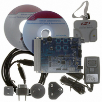
DEV KIT FOR C8051F700
Manufacturer
Silicon Laboratories Inc
Type
MCUr
Datasheets
1.C8051F700-TB.pdf
(1 pages)
2.C8051F700-TB.pdf
(306 pages)
3.C8051F700-TB.pdf
(18 pages)
Specifications of C8051F700DK
Contents
Board, Cables, CD, Debugger, Power Supply
Processor To Be Evaluated
C8051F7x
Processor Series
C8051F7xx
Interface Type
USB
Operating Supply Voltage
3.3 V
Lead Free Status / RoHS Status
Lead free / RoHS Compliant
For Use With/related Products
C8051F7xx
Lead Free Status / Rohs Status
Lead free / RoHS Compliant
Other names
336-1635


C8051F70x/71x
29. Cyclic Redundancy Check Unit (CRC0)............................................................. 211
30. SMBus................................................................................................................... 219
31. Enhanced Serial Peripheral Interface (SPI0) ..................................................... 241
6
28.3. Priority Crossbar Decoder ............................................................................. 185
28.4. Port I/O Initialization ...................................................................................... 189
28.5. Port Match ..................................................................................................... 192
28.6. Special Function Registers for Accessing and Configuring Port I/O ............. 194
29.1. 16-bit CRC Algorithm..................................................................................... 212
29.2. 32-bit CRC Algorithm..................................................................................... 213
29.3. Preparing for a CRC Calculation ................................................................... 214
29.4. Performing a CRC Calculation ...................................................................... 214
29.5. Accessing the CRC0 Result .......................................................................... 214
29.6. CRC0 Bit Reverse Feature............................................................................ 218
30.1. Supporting Documents .................................................................................. 220
30.2. SMBus Configuration..................................................................................... 220
30.3. SMBus Operation .......................................................................................... 220
30.4. Using the SMBus........................................................................................... 222
30.5. SMBus Transfer Modes................................................................................. 232
30.6. SMBus Status Decoding................................................................................ 235
31.1. Signal Descriptions........................................................................................ 242
31.2. SPI0 Master Mode Operation ........................................................................ 242
31.3. SPI0 Slave Mode Operation .......................................................................... 244
31.4. SPI0 Interrupt Sources .................................................................................. 245
28.2.1. Assigning Port I/O Pins to Analog Functions ........................................ 182
28.2.2. Assigning Port I/O Pins to Digital Functions.......................................... 184
28.2.3. Assigning Port I/O Pins to External Event Trigger Functions................ 184
30.3.1. Transmitter Vs. Receiver....................................................................... 221
30.3.2. Arbitration.............................................................................................. 221
30.3.3. Clock Low Extension............................................................................. 221
30.3.4. SCL Low Timeout.................................................................................. 221
30.3.5. SCL High (SMBus Free) Timeout ......................................................... 222
30.4.1. SMBus Configuration Register.............................................................. 222
30.4.2. SMB0CN Control Register .................................................................... 226
30.4.3. Hardware Slave Address Recognition .................................................. 228
30.4.4. Data Register ........................................................................................ 231
30.5.1. Write Sequence (Master) ...................................................................... 232
30.5.2. Read Sequence (Master) ...................................................................... 233
30.5.3. Write Sequence (Slave) ........................................................................ 234
30.5.4. Read Sequence (Slave) ........................................................................ 235
31.1.1. Master Out, Slave In (MOSI)................................................................. 242
31.1.2. Master In, Slave Out (MISO)................................................................. 242
31.1.3. Serial Clock (SCK) ................................................................................ 242
31.1.4. Slave Select (NSS) ............................................................................... 242
30.4.2.1. Software ACK Generation ............................................................ 226
30.4.2.2. Hardware ACK Generation ........................................................... 226
Rev. 1.0
Related parts for C8051F700DK
Image
Part Number
Description
Manufacturer
Datasheet
Request
R

Part Number:
Description:
SMD/C°/SINGLE-ENDED OUTPUT SILICON OSCILLATOR
Manufacturer:
Silicon Laboratories Inc
Part Number:
Description:
Manufacturer:
Silicon Laboratories Inc
Datasheet:
Part Number:
Description:
N/A N/A/SI4010 AES KEYFOB DEMO WITH LCD RX
Manufacturer:
Silicon Laboratories Inc
Datasheet:
Part Number:
Description:
N/A N/A/SI4010 SIMPLIFIED KEY FOB DEMO WITH LED RX
Manufacturer:
Silicon Laboratories Inc
Datasheet:
Part Number:
Description:
N/A/-40 TO 85 OC/EZLINK MODULE; F930/4432 HIGH BAND (REV E/B1)
Manufacturer:
Silicon Laboratories Inc
Part Number:
Description:
EZLink Module; F930/4432 Low Band (rev e/B1)
Manufacturer:
Silicon Laboratories Inc
Part Number:
Description:
I°/4460 10 DBM RADIO TEST CARD 434 MHZ
Manufacturer:
Silicon Laboratories Inc
Part Number:
Description:
I°/4461 14 DBM RADIO TEST CARD 868 MHZ
Manufacturer:
Silicon Laboratories Inc
Part Number:
Description:
I°/4463 20 DBM RFSWITCH RADIO TEST CARD 460 MHZ
Manufacturer:
Silicon Laboratories Inc
Part Number:
Description:
I°/4463 20 DBM RADIO TEST CARD 868 MHZ
Manufacturer:
Silicon Laboratories Inc
Part Number:
Description:
I°/4463 27 DBM RADIO TEST CARD 868 MHZ
Manufacturer:
Silicon Laboratories Inc
Part Number:
Description:
I°/4463 SKYWORKS 30 DBM RADIO TEST CARD 915 MHZ
Manufacturer:
Silicon Laboratories Inc
Part Number:
Description:
N/A N/A/-40 TO 85 OC/4463 RFMD 30 DBM RADIO TEST CARD 915 MHZ
Manufacturer:
Silicon Laboratories Inc
Part Number:
Description:
I°/4463 20 DBM RADIO TEST CARD 169 MHZ
Manufacturer:
Silicon Laboratories Inc