C8051F700DK Silicon Laboratories Inc, C8051F700DK Datasheet - Page 28
C8051F700DK
Manufacturer Part Number
C8051F700DK
Description
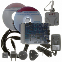
DEV KIT FOR C8051F700
Manufacturer
Silicon Laboratories Inc
Type
MCUr
Datasheets
1.C8051F700-TB.pdf
(1 pages)
2.C8051F700-TB.pdf
(306 pages)
3.C8051F700-TB.pdf
(18 pages)
Specifications of C8051F700DK
Contents
Board, Cables, CD, Debugger, Power Supply
Processor To Be Evaluated
C8051F7x
Processor Series
C8051F7xx
Interface Type
USB
Operating Supply Voltage
3.3 V
Lead Free Status / RoHS Status
Lead free / RoHS Compliant
For Use With/related Products
C8051F7xx
Lead Free Status / Rohs Status
Lead free / RoHS Compliant
Other names
336-1635


C8051F70x/71x
3. Pin Definitions
28
XTAL1
XTAL2
AGND
Name TQFP64 TQFP48
C2CK
VREF
RST /
P0.0 /
P0.2 /
P0.3 /
P0.1/
GND
P0.4
P0.5
P0.6
C2D
V
DD
41, 57
40, 56
8, 24,
9, 25,
58
59
55
54
53
52
51
50
49
8, 20, 44
QFN48
30, 43
9, 21,
45
46
42
41
40
39
38
37
36
Table 3.1. Pin Definitions for the C8051F70x/71x
QFN32 QFN24
Center
27
28
29
26
25
24
—
—
—
—
21
20
22
23
—
—
—
—
19
18
—
D I/O or
D I/O or
D I/O or
D I/O or
D I/O or
D I/O or
D I/O or
A I/O or
Rev. 1.0
D I/O
D I/O
D I/O
Type
A In
A In
A In
A In
A In
A In
D In
A In
A In
A In
Power Supply Voltage.
Ground.
Device Reset. Open-drain output of internal
POR or V
Clock signal for the C2 Debug Interface.
Bi-directional data signal for the C2 Debug
Interface.
Port 0.0.
ADC0 Input.
External VREF input.
Port 0.1.
ADC0 Input.
External AGND input.
Port 0.2.
ADC0 Input.
External Clock Pin. This pin can be used for
crystal clock mode.
Port 0.3.
ADC0 Input.
External Clock Pin. This pin can be used for
RC, crystal, and CMOS clock modes.
Port 0.4.
ADC0 Input.
Port 0.5.
ADC0 Input.
Port 0.6.
ADC0 Input.
DD
monitor.
Description
Related parts for C8051F700DK
Image
Part Number
Description
Manufacturer
Datasheet
Request
R

Part Number:
Description:
SMD/C°/SINGLE-ENDED OUTPUT SILICON OSCILLATOR
Manufacturer:
Silicon Laboratories Inc
Part Number:
Description:
Manufacturer:
Silicon Laboratories Inc
Datasheet:
Part Number:
Description:
N/A N/A/SI4010 AES KEYFOB DEMO WITH LCD RX
Manufacturer:
Silicon Laboratories Inc
Datasheet:
Part Number:
Description:
N/A N/A/SI4010 SIMPLIFIED KEY FOB DEMO WITH LED RX
Manufacturer:
Silicon Laboratories Inc
Datasheet:
Part Number:
Description:
N/A/-40 TO 85 OC/EZLINK MODULE; F930/4432 HIGH BAND (REV E/B1)
Manufacturer:
Silicon Laboratories Inc
Part Number:
Description:
EZLink Module; F930/4432 Low Band (rev e/B1)
Manufacturer:
Silicon Laboratories Inc
Part Number:
Description:
I°/4460 10 DBM RADIO TEST CARD 434 MHZ
Manufacturer:
Silicon Laboratories Inc
Part Number:
Description:
I°/4461 14 DBM RADIO TEST CARD 868 MHZ
Manufacturer:
Silicon Laboratories Inc
Part Number:
Description:
I°/4463 20 DBM RFSWITCH RADIO TEST CARD 460 MHZ
Manufacturer:
Silicon Laboratories Inc
Part Number:
Description:
I°/4463 20 DBM RADIO TEST CARD 868 MHZ
Manufacturer:
Silicon Laboratories Inc
Part Number:
Description:
I°/4463 27 DBM RADIO TEST CARD 868 MHZ
Manufacturer:
Silicon Laboratories Inc
Part Number:
Description:
I°/4463 SKYWORKS 30 DBM RADIO TEST CARD 915 MHZ
Manufacturer:
Silicon Laboratories Inc
Part Number:
Description:
N/A N/A/-40 TO 85 OC/4463 RFMD 30 DBM RADIO TEST CARD 915 MHZ
Manufacturer:
Silicon Laboratories Inc
Part Number:
Description:
I°/4463 20 DBM RADIO TEST CARD 169 MHZ
Manufacturer:
Silicon Laboratories Inc