C8051F700DK Silicon Laboratories Inc, C8051F700DK Datasheet - Page 5
C8051F700DK
Manufacturer Part Number
C8051F700DK
Description
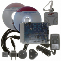
DEV KIT FOR C8051F700
Manufacturer
Silicon Laboratories Inc
Type
MCUr
Datasheets
1.C8051F700-TB.pdf
(1 pages)
2.C8051F700-TB.pdf
(306 pages)
3.C8051F700-TB.pdf
(18 pages)
Specifications of C8051F700DK
Contents
Board, Cables, CD, Debugger, Power Supply
Processor To Be Evaluated
C8051F7x
Processor Series
C8051F7xx
Interface Type
USB
Operating Supply Voltage
3.3 V
Lead Free Status / RoHS Status
Lead free / RoHS Compliant
For Use With/related Products
C8051F7xx
Lead Free Status / Rohs Status
Lead free / RoHS Compliant
Other names
336-1635


23. EEPROM ............................................................................................................... 155
24. Power Management Modes................................................................................. 160
25. Reset Sources ...................................................................................................... 163
26. Watchdog Timer................................................................................................... 169
27. Oscillators and Clock Selection ......................................................................... 171
28. Port Input/Output ................................................................................................. 180
22.2. Non-volatile Data Storage ............................................................................. 149
22.3. Security Options ............................................................................................ 149
22.4. Flash Write and Erase Guidelines ................................................................. 150
23.1. RAM Reads and Writes ................................................................................. 155
23.2. Auto Increment .............................................................................................. 155
23.3. Interfacing with the EEPROM........................................................................ 155
23.4. EEPROM Security ......................................................................................... 156
24.1. Idle Mode....................................................................................................... 160
24.2. Stop Mode ..................................................................................................... 161
24.3. Suspend Mode .............................................................................................. 161
25.1. Power-On Reset ............................................................................................ 164
25.2. Power-Fail Reset / VDD Monitor ................................................................... 165
25.3. External Reset ............................................................................................... 166
25.4. Missing Clock Detector Reset ....................................................................... 166
25.5. Comparator0 Reset ....................................................................................... 167
25.6. Watchdog Timer Reset.................................................................................. 167
25.7. Flash Error Reset .......................................................................................... 167
25.8. Software Reset .............................................................................................. 167
26.1. Enable/Reset WDT........................................................................................ 169
26.2. Disable WDT ................................................................................................. 169
26.3. Disable WDT Lockout.................................................................................... 169
26.4. Setting WDT Interval ..................................................................................... 169
27.1. System Clock Selection................................................................................. 171
27.2. Programmable Internal High-Frequency (H-F) Oscillator .............................. 173
27.3. External Oscillator Drive Circuit..................................................................... 175
28.1. Port I/O Modes of Operation.......................................................................... 181
28.2. Assigning Port I/O Pins to Analog and Digital Functions............................... 182
22.1.2. Flash Erase Procedure ......................................................................... 148
22.1.3. Flash Write Procedure .......................................................................... 149
22.4.1. VDD Maintenance and the VDD Monitor .............................................. 151
22.4.2. PSWE Maintenance .............................................................................. 151
22.4.3. System Clock ........................................................................................ 152
27.3.1. External Crystal Example...................................................................... 177
27.3.2. External RC Example............................................................................ 178
27.3.3. External Capacitor Example.................................................................. 179
28.1.1. Port Pins Configured for Analog I/O...................................................... 181
28.1.2. Port Pins Configured For Digital I/O...................................................... 181
28.1.3. Interfacing Port I/O to 5 V Logic ............................................................ 182
28.1.4. Increasing Port I/O Drive Strength ........................................................ 182
Rev. 1.0
C8051F70x/71x
5
Related parts for C8051F700DK
Image
Part Number
Description
Manufacturer
Datasheet
Request
R

Part Number:
Description:
SMD/C°/SINGLE-ENDED OUTPUT SILICON OSCILLATOR
Manufacturer:
Silicon Laboratories Inc
Part Number:
Description:
Manufacturer:
Silicon Laboratories Inc
Datasheet:
Part Number:
Description:
N/A N/A/SI4010 AES KEYFOB DEMO WITH LCD RX
Manufacturer:
Silicon Laboratories Inc
Datasheet:
Part Number:
Description:
N/A N/A/SI4010 SIMPLIFIED KEY FOB DEMO WITH LED RX
Manufacturer:
Silicon Laboratories Inc
Datasheet:
Part Number:
Description:
N/A/-40 TO 85 OC/EZLINK MODULE; F930/4432 HIGH BAND (REV E/B1)
Manufacturer:
Silicon Laboratories Inc
Part Number:
Description:
EZLink Module; F930/4432 Low Band (rev e/B1)
Manufacturer:
Silicon Laboratories Inc
Part Number:
Description:
I°/4460 10 DBM RADIO TEST CARD 434 MHZ
Manufacturer:
Silicon Laboratories Inc
Part Number:
Description:
I°/4461 14 DBM RADIO TEST CARD 868 MHZ
Manufacturer:
Silicon Laboratories Inc
Part Number:
Description:
I°/4463 20 DBM RFSWITCH RADIO TEST CARD 460 MHZ
Manufacturer:
Silicon Laboratories Inc
Part Number:
Description:
I°/4463 20 DBM RADIO TEST CARD 868 MHZ
Manufacturer:
Silicon Laboratories Inc
Part Number:
Description:
I°/4463 27 DBM RADIO TEST CARD 868 MHZ
Manufacturer:
Silicon Laboratories Inc
Part Number:
Description:
I°/4463 SKYWORKS 30 DBM RADIO TEST CARD 915 MHZ
Manufacturer:
Silicon Laboratories Inc
Part Number:
Description:
N/A N/A/-40 TO 85 OC/4463 RFMD 30 DBM RADIO TEST CARD 915 MHZ
Manufacturer:
Silicon Laboratories Inc
Part Number:
Description:
I°/4463 20 DBM RADIO TEST CARD 169 MHZ
Manufacturer:
Silicon Laboratories Inc