C8051F700DK Silicon Laboratories Inc, C8051F700DK Datasheet - Page 103
C8051F700DK
Manufacturer Part Number
C8051F700DK
Description
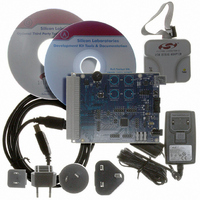
DEV KIT FOR C8051F700
Manufacturer
Silicon Laboratories Inc
Type
MCUr
Datasheets
1.C8051F700-TB.pdf
(1 pages)
2.C8051F700-TB.pdf
(306 pages)
3.C8051F700-TB.pdf
(18 pages)
Specifications of C8051F700DK
Contents
Board, Cables, CD, Debugger, Power Supply
Processor To Be Evaluated
C8051F7x
Processor Series
C8051F7xx
Interface Type
USB
Operating Supply Voltage
3.3 V
Lead Free Status / RoHS Status
Lead free / RoHS Compliant
For Use With/related Products
C8051F7xx
Lead Free Status / Rohs Status
Lead free / RoHS Compliant
Other names
336-1635


C8051F70x/71x
Notes on Registers, Operands and Addressing Modes:
Rn—Register R0–R7 of the currently selected register bank.
@Ri—Data RAM location addressed indirectly through R0 or R1.
rel—8-bit, signed (twos complement) offset relative to the first byte of the following instruction. Used by
SJMP and all conditional jumps.
direct—8-bit internal data location’s address. This could be a direct-access Data RAM location (0x00–
0x7F) or an SFR (0x80–0xFF).
#data—8-bit constant
#data16—16-bit constant
bit—Direct-accessed bit in Data RAM or SFR
addr11—11-bit destination address used by ACALL and AJMP. The destination must be within the
same 2 kB page of program memory as the first byte of the following instruction.
addr16—16-bit destination address used by LCALL and LJMP. The destination may be anywhere within
the 8 kB program memory space.
There is one unused opcode (0xA5) that performs the same function as NOP.
All mnemonics copyrighted © Intel Corporation 1980.
Rev. 1.0
103
Related parts for C8051F700DK
Image
Part Number
Description
Manufacturer
Datasheet
Request
R

Part Number:
Description:
SMD/C°/SINGLE-ENDED OUTPUT SILICON OSCILLATOR
Manufacturer:
Silicon Laboratories Inc
Part Number:
Description:
Manufacturer:
Silicon Laboratories Inc
Datasheet:
Part Number:
Description:
N/A N/A/SI4010 AES KEYFOB DEMO WITH LCD RX
Manufacturer:
Silicon Laboratories Inc
Datasheet:
Part Number:
Description:
N/A N/A/SI4010 SIMPLIFIED KEY FOB DEMO WITH LED RX
Manufacturer:
Silicon Laboratories Inc
Datasheet:
Part Number:
Description:
N/A/-40 TO 85 OC/EZLINK MODULE; F930/4432 HIGH BAND (REV E/B1)
Manufacturer:
Silicon Laboratories Inc
Part Number:
Description:
EZLink Module; F930/4432 Low Band (rev e/B1)
Manufacturer:
Silicon Laboratories Inc
Part Number:
Description:
I°/4460 10 DBM RADIO TEST CARD 434 MHZ
Manufacturer:
Silicon Laboratories Inc
Part Number:
Description:
I°/4461 14 DBM RADIO TEST CARD 868 MHZ
Manufacturer:
Silicon Laboratories Inc
Part Number:
Description:
I°/4463 20 DBM RFSWITCH RADIO TEST CARD 460 MHZ
Manufacturer:
Silicon Laboratories Inc
Part Number:
Description:
I°/4463 20 DBM RADIO TEST CARD 868 MHZ
Manufacturer:
Silicon Laboratories Inc
Part Number:
Description:
I°/4463 27 DBM RADIO TEST CARD 868 MHZ
Manufacturer:
Silicon Laboratories Inc
Part Number:
Description:
I°/4463 SKYWORKS 30 DBM RADIO TEST CARD 915 MHZ
Manufacturer:
Silicon Laboratories Inc
Part Number:
Description:
N/A N/A/-40 TO 85 OC/4463 RFMD 30 DBM RADIO TEST CARD 915 MHZ
Manufacturer:
Silicon Laboratories Inc
Part Number:
Description:
I°/4463 20 DBM RADIO TEST CARD 169 MHZ
Manufacturer:
Silicon Laboratories Inc