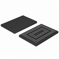
SSTUB32865ET/G,518 NXP Semiconductors, SSTUB32865ET/G,518 Datasheet - Page 9

SSTUB32865ET/G,518
Manufacturer Part Number
SSTUB32865ET/G,518
Description
IC REG BUFFER 28BIT 160TFBGA
Manufacturer
NXP Semiconductors
Datasheet
1.SSTUB32865ETG518.pdf
(28 pages)
Specifications of SSTUB32865ET/G,518
Logic Type
1:2 Registered Buffer with Parity
Supply Voltage
1.7 V ~ 2 V
Number Of Bits
28
Operating Temperature
0°C ~ 70°C
Mounting Type
Surface Mount
Package / Case
160-TFBGA
Logic Family
SSTU
Logical Function
Reg Bfr W/ParityTst
Number Of Elements
1
Number Of Inputs
28
Number Of Outputs
56
High Level Output Current
-8mA
Low Level Output Current
8mA
Propagation Delay Time
3ns
Operating Supply Voltage (typ)
1.8V
Operating Supply Voltage (max)
2V
Operating Supply Voltage (min)
1.7V
Clock-edge Trigger Type
Posit/Negat-Edge
Polarity
Non-Inverting
Technology
CMOS
Frequency (max)
450(Min)MHz
Mounting
Surface Mount
Pin Count
160
Operating Temp Range
0C to 70C
Operating Temperature Classification
Commercial
Lead Free Status / RoHS Status
Lead free / RoHS Compliant
Other names
568-3542-2
935281691518
SSTUB32865ET/G-T
935281691518
SSTUB32865ET/G-T
Available stocks
Company
Part Number
Manufacturer
Quantity
Price
Company:
Part Number:
SSTUB32865ET/G,518
Manufacturer:
NXP Semiconductors
Quantity:
10 000
NXP Semiconductors
[1]
[2]
[3]
[4]
SSTUB32865_3
Product data sheet
DCS2 and DCS3 operate identically to DCS0 and DCS1 with regard to the parity function.
PARIN arrives one clock cycle after the data to which it applies. All Dn inputs must be driven to a known state for parity to be calculated
correctly.
This condition assumes PTYERR is HIGH at the crossing of CK going HIGH and CK going LOW. If PTYERR is LOW, it stays latched
LOW for two clock cycles or until RESET is driven LOW. CSGATEEN is ‘don’t care’ for PTYERR.
PTYERR
0
is the previous state of output PTYERR.
7.2 Functional information
Table 6.
This 28-bit 1 : 2 registered buffer with parity is designed for 1.7 V to 2.0 V V
All clock and data inputs are compatible with the JEDEC standard for SSTL_18. The
control inputs are LVCMOS. All outputs are 1.8 V CMOS drivers that have been optimized
to drive the DDR2 DIMM load.
The SSTUB32865 operates from a differential clock (CK and CK). Data are registered at
the crossing of CK going HIGH, and CK going LOW.
A programming pin, SELDR, allows the user to select between two drive strength options
by tying this pin either LOW or HIGH on the DIMM. The truth table for these options is
shown in
The device supports low-power standby operation. When the reset input (RESET) is LOW,
the differential input receivers are disabled, and undriven (floating) data, clock and
reference voltage (VREF) inputs are allowed. In addition, when RESET is LOW all
registers are reset, and all outputs except PTYERR are forced LOW. The LVCMOS
RESET input must always be held at a valid logic HIGH or LOW level.
To ensure defined outputs from the register before a stable clock has been supplied,
RESET must be held in the LOW state during power-up.
In the DDR2 RDIMM application, RESET is specified to be completely asynchronous with
respect to CK and CK. Therefore, no timing relationship can be guaranteed between the
two. When entering reset, the register will be cleared and the data outputs will be driven
LOW quickly, relative to the time to disable the differential input receivers. However, when
coming out of reset, the register will become active quickly, relative to the time to enable
the differential input receivers. As long as the data inputs are LOW, and the clock is stable
during the time from the LOW-to-HIGH transition of RESET until the input receivers are
fully enabled, the design of the SSTUB32865 ensures that the outputs remain LOW, thus
ensuring no glitches on the output.
The device monitors DCS0, DCS1, DCS2 and DCS3 inputs and will gate the Qn outputs
from changing states when all DCSn inputs are HIGH. If DCSn input is LOW, the Qn
outputs will function normally. The RESET input has priority over the DCSn control and
will force the Qn outputs LOW and the PTYERR output HIGH. If the DCSn-control
Input
SELDR
L
H
Table
Truth table SELDR
6.
Mode
high output drive
normal output drive
Rev. 03 — 27 March 2007
1.8 V DDR2-800 registered buffer with parity
SSTUB32865
© NXP B.V. 2007. All rights reserved.
DD
operation.
9 of 28


