SSTUB32865ET/G,518 NXP Semiconductors, SSTUB32865ET/G,518 Datasheet - Page 2
SSTUB32865ET/G,518
Manufacturer Part Number
SSTUB32865ET/G,518
Description
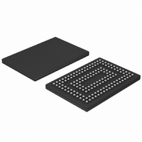
IC REG BUFFER 28BIT 160TFBGA
Manufacturer
NXP Semiconductors
Datasheet
1.SSTUB32865ETG518.pdf
(28 pages)
Specifications of SSTUB32865ET/G,518
Logic Type
1:2 Registered Buffer with Parity
Supply Voltage
1.7 V ~ 2 V
Number Of Bits
28
Operating Temperature
0°C ~ 70°C
Mounting Type
Surface Mount
Package / Case
160-TFBGA
Logic Family
SSTU
Logical Function
Reg Bfr W/ParityTst
Number Of Elements
1
Number Of Inputs
28
Number Of Outputs
56
High Level Output Current
-8mA
Low Level Output Current
8mA
Propagation Delay Time
3ns
Operating Supply Voltage (typ)
1.8V
Operating Supply Voltage (max)
2V
Operating Supply Voltage (min)
1.7V
Clock-edge Trigger Type
Posit/Negat-Edge
Polarity
Non-Inverting
Technology
CMOS
Frequency (max)
450(Min)MHz
Mounting
Surface Mount
Pin Count
160
Operating Temp Range
0C to 70C
Operating Temperature Classification
Commercial
Lead Free Status / RoHS Status
Lead free / RoHS Compliant
Other names
568-3542-2
935281691518
SSTUB32865ET/G-T
935281691518
SSTUB32865ET/G-T
Available stocks
Company
Part Number
Manufacturer
Quantity
Price
Company:

Part Number:
SSTUB32865ET/G,518
Manufacturer:
NXP Semiconductors
Quantity:
10 000


NXP Semiconductors
3. Applications
4. Ordering information
Table 1.
SSTUB32865_3
Product data sheet
Type number
SSTUB32865ET/G
SSTUB32865ET/S
Ordering information
4.1 Ordering options
Solder process
Pb-free (SnAgCu solder ball
compound)
Pb-free (SnAgCu solder ball
compound)
I
I
I
I
I
I
I
I
I
Table 2.
Type number
SSTUB32865ET/G
SSTUB32865ET/S
Chip-selects minimize power consumption by gating data outputs from changing state
Two additional chip select inputs allow optional flexible enabling and disabling
Supports Stub Series Terminated Logic SSTL_18 data inputs
Differential clock (CK and CK) inputs
Supports LVCMOS switching levels on the control and RESET inputs
Single 1.8 V supply operation (1.7 V to 2.0 V)
Available in 160-ball 9 mm
400 MT/s to 800 MT/s high-density (for example, 2 rank by 4) DDR2 registered DIMMs
DDR2 Registered DIMMs (RDIMM) desiring parity checking functionality
Ordering options
Rev. 03 — 27 March 2007
Temperature range
T
T
amb
amb
Package
Name
TFBGA160 plastic thin fine-pitch ball grid array package;
TFBGA160 plastic thin fine-pitch ball grid array package;
= 0 C to +70 C
= 0 C to +85 C
13 mm, 0.65 mm ball pitch TFBGA package
Description
160 balls; body 9
160 balls; body 9
1.8 V DDR2-800 registered buffer with parity
13
13
0.7 mm
0.7 mm
SSTUB32865
© NXP B.V. 2007. All rights reserved.
Version
SOT802-2
SOT802-2
2 of 28
Related parts for SSTUB32865ET/G,518
Image
Part Number
Description
Manufacturer
Datasheet
Request
R

Part Number:
Description:
Sstub32865 1.8 V 28-bit 1 2 Registered Buffer With Parity For Ddr2-800 Rdimm Applications
Manufacturer:
NXP Semiconductors
Datasheet:
Part Number:
Description:
NXP Semiconductors designed the LPC2420/2460 microcontroller around a 16-bit/32-bitARM7TDMI-S CPU core with real-time debug interfaces that include both JTAG andembedded trace
Manufacturer:
NXP Semiconductors
Datasheet:

Part Number:
Description:
NXP Semiconductors designed the LPC2458 microcontroller around a 16-bit/32-bitARM7TDMI-S CPU core with real-time debug interfaces that include both JTAG andembedded trace
Manufacturer:
NXP Semiconductors
Datasheet:
Part Number:
Description:
NXP Semiconductors designed the LPC2468 microcontroller around a 16-bit/32-bitARM7TDMI-S CPU core with real-time debug interfaces that include both JTAG andembedded trace
Manufacturer:
NXP Semiconductors
Datasheet:
Part Number:
Description:
NXP Semiconductors designed the LPC2470 microcontroller, powered by theARM7TDMI-S core, to be a highly integrated microcontroller for a wide range ofapplications that require advanced communications and high quality graphic displays
Manufacturer:
NXP Semiconductors
Datasheet:
Part Number:
Description:
NXP Semiconductors designed the LPC2478 microcontroller, powered by theARM7TDMI-S core, to be a highly integrated microcontroller for a wide range ofapplications that require advanced communications and high quality graphic displays
Manufacturer:
NXP Semiconductors
Datasheet:
Part Number:
Description:
The Philips Semiconductors XA (eXtended Architecture) family of 16-bit single-chip microcontrollers is powerful enough to easily handle the requirements of high performance embedded applications, yet inexpensive enough to compete in the market for hi
Manufacturer:
NXP Semiconductors
Datasheet:
Part Number:
Description:
The XA-S3 device is a member of Philips Semiconductors? XA(eXtended Architecture) family of high performance 16-bitsingle-chip microcontrollers
Manufacturer:
NXP Semiconductors
Datasheet:

Part Number:
Description:
The NXP BlueStreak LH75401/LH75411 family consists of two low-cost 16/32-bit System-on-Chip (SoC) devices
Manufacturer:
NXP Semiconductors
Datasheet:
Part Number:
Description:
The NXP LPC3130/3131 combine an 180 MHz ARM926EJ-S CPU core, high-speed USB2
Manufacturer:
NXP Semiconductors
Datasheet:
Part Number:
Description:
The NXP LPC3141 combine a 270 MHz ARM926EJ-S CPU core, High-speed USB 2
Manufacturer:
NXP Semiconductors
Part Number:
Description:
The NXP LPC3143 combine a 270 MHz ARM926EJ-S CPU core, High-speed USB 2
Manufacturer:
NXP Semiconductors

Part Number:
Description:
The NXP LPC3152 combines an 180 MHz ARM926EJ-S CPU core, High-speed USB 2
Manufacturer:
NXP Semiconductors
Part Number:
Description:
The NXP LPC3154 combines an 180 MHz ARM926EJ-S CPU core, High-speed USB 2
Manufacturer:
NXP Semiconductors