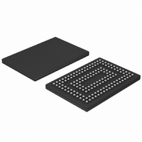
SSTUB32865ET/G,518 NXP Semiconductors, SSTUB32865ET/G,518 Datasheet - Page 10

SSTUB32865ET/G,518
Manufacturer Part Number
SSTUB32865ET/G,518
Description
IC REG BUFFER 28BIT 160TFBGA
Manufacturer
NXP Semiconductors
Datasheet
1.SSTUB32865ETG518.pdf
(28 pages)
Specifications of SSTUB32865ET/G,518
Logic Type
1:2 Registered Buffer with Parity
Supply Voltage
1.7 V ~ 2 V
Number Of Bits
28
Operating Temperature
0°C ~ 70°C
Mounting Type
Surface Mount
Package / Case
160-TFBGA
Logic Family
SSTU
Logical Function
Reg Bfr W/ParityTst
Number Of Elements
1
Number Of Inputs
28
Number Of Outputs
56
High Level Output Current
-8mA
Low Level Output Current
8mA
Propagation Delay Time
3ns
Operating Supply Voltage (typ)
1.8V
Operating Supply Voltage (max)
2V
Operating Supply Voltage (min)
1.7V
Clock-edge Trigger Type
Posit/Negat-Edge
Polarity
Non-Inverting
Technology
CMOS
Frequency (max)
450(Min)MHz
Mounting
Surface Mount
Pin Count
160
Operating Temp Range
0C to 70C
Operating Temperature Classification
Commercial
Lead Free Status / RoHS Status
Lead free / RoHS Compliant
Other names
568-3542-2
935281691518
SSTUB32865ET/G-T
935281691518
SSTUB32865ET/G-T
Available stocks
Company
Part Number
Manufacturer
Quantity
Price
Company:
Part Number:
SSTUB32865ET/G,518
Manufacturer:
NXP Semiconductors
Quantity:
10 000
NXP Semiconductors
SSTUB32865_3
Product data sheet
7.3.1 Chip Select (CS) gating of key inputs (DCS0, DCS1, DCS2, DCS3,
7.3.2 Parity error checking and reporting
7.3.3 Reset (RESET)
7.3 Functional differences to SSTU32864
functionality is not desired, then the CSGATEEN input can be hardwired to ground, in
which case, the set-up time requirement for DCSn would be the same as for the other Dn
data inputs.
The SSTUB32865 includes a parity checking function. The SSTUB32865 accepts a parity
bit from the memory controller at its input pin PARIN, compares it with the data received
on the Dn inputs (with either DCSn inputs active) and indicates whether a parity error has
occurred on its open-drain PTYERR pin (active LOW).
The SSTUB32865 for its basic register functionality, signal definition and performance is
based upon the industry-standard SSTU32864, but provides key operational features
which differ (at least in part) from the industry-standard register in the following aspects:
CSGATEEN)
As a means to reduce device power, the internal latches will only be updated when one or
more of the CS inputs are active (LOW) and CSGATEEN HIGH at the rising edge of the
clock. The 22 ‘Chip-Select-gated’ input signals associated with this function include
addresses (ADDR0 to ADDR15, BA0 to BA2), and RAS, CAS, WE, with the remaining
signals (CS, CKE, ODT) continuously re-driven at the rising edge of every clock as they
are independent of CS. The CS gating function can be disabled by tying CSGATEEN
LOW, enabling all internal latches to be updated on every rising edge of the clock.
Table 7.
The SSTUB32865 incorporates a parity function, whereby the signal received on input pin
PARIN is received as parity to the register, one clock cycle later than the CS-gated inputs.
The received parity bit is then compared to the parity calculated across these same inputs
by the register parity logic to verify that the information has not been corrupted. The 22
CS-gated input signals will be latched and re-driven on the first clock, and any error will be
reported one clock cycle later via the PTYERR output pin (driven LOW for two consecutive
clock cycles). PTYERR is an open-drain output, allowing multiple modules to share a
common signal pin for reporting the occurrence of a parity error during a valid command
cycle (coincident with the re-driven signals). This output is driven LOW for two consecutive
clock cycles to allow the memory controller sufficient time to sense and capture the error
even. A LOW state on PTYERR indicates that a parity error has occurred.
Similar to the RESET pin on the industry-standard SSTU32864, this pin is used to clear all
internal latches and all outputs will be driven LOW quickly except the PTYERR output,
which will be floated (and will normally default HIGH by their external pull-up).
Mode
Gating
Non-gating
Chip Select gating mode
Signal name
CSGATEEN
HIGH
CSGATEEN
LOW
Rev. 03 — 27 March 2007
Description
Registers only re-drive signals to the DRAMs when
Chip Select inputs are LOW.
Registers always re-drive signals on every clock cycle,
independent of the state of the Chip Select inputs.
1.8 V DDR2-800 registered buffer with parity
SSTUB32865
© NXP B.V. 2007. All rights reserved.
10 of 28


