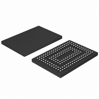
SSTUB32865ET/G,518 NXP Semiconductors, SSTUB32865ET/G,518 Datasheet - Page 24

SSTUB32865ET/G,518
Manufacturer Part Number
SSTUB32865ET/G,518
Description
IC REG BUFFER 28BIT 160TFBGA
Manufacturer
NXP Semiconductors
Datasheet
1.SSTUB32865ETG518.pdf
(28 pages)
Specifications of SSTUB32865ET/G,518
Logic Type
1:2 Registered Buffer with Parity
Supply Voltage
1.7 V ~ 2 V
Number Of Bits
28
Operating Temperature
0°C ~ 70°C
Mounting Type
Surface Mount
Package / Case
160-TFBGA
Logic Family
SSTU
Logical Function
Reg Bfr W/ParityTst
Number Of Elements
1
Number Of Inputs
28
Number Of Outputs
56
High Level Output Current
-8mA
Low Level Output Current
8mA
Propagation Delay Time
3ns
Operating Supply Voltage (typ)
1.8V
Operating Supply Voltage (max)
2V
Operating Supply Voltage (min)
1.7V
Clock-edge Trigger Type
Posit/Negat-Edge
Polarity
Non-Inverting
Technology
CMOS
Frequency (max)
450(Min)MHz
Mounting
Surface Mount
Pin Count
160
Operating Temp Range
0C to 70C
Operating Temperature Classification
Commercial
Lead Free Status / RoHS Status
Lead free / RoHS Compliant
Other names
568-3542-2
935281691518
SSTUB32865ET/G-T
935281691518
SSTUB32865ET/G-T
Available stocks
Company
Part Number
Manufacturer
Quantity
Price
Company:
Part Number:
SSTUB32865ET/G,518
Manufacturer:
NXP Semiconductors
Quantity:
10 000
NXP Semiconductors
13. Soldering
SSTUB32865_3
Product data sheet
13.1 Introduction to soldering
13.2 Wave and reflow soldering
13.3 Wave soldering
This text provides a very brief insight into a complex technology. A more in-depth account
of soldering ICs can be found in Application Note AN10365 “Surface mount reflow
soldering description” .
Soldering is one of the most common methods through which packages are attached to
Printed Circuit Boards (PCBs), to form electrical circuits. The soldered joint provides both
the mechanical and the electrical connection. There is no single soldering method that is
ideal for all IC packages. Wave soldering is often preferred when through-hole and
Surface Mount Devices (SMDs) are mixed on one printed wiring board; however, it is not
suitable for fine pitch SMDs. Reflow soldering is ideal for the small pitches and high
densities that come with increased miniaturization.
Wave soldering is a joining technology in which the joints are made by solder coming from
a standing wave of liquid solder. The wave soldering process is suitable for the following:
Not all SMDs can be wave soldered. Packages with solder balls, and some leadless
packages which have solder lands underneath the body, cannot be wave soldered. Also,
leaded SMDs with leads having a pitch smaller than ~0.6 mm cannot be wave soldered,
due to an increased probability of bridging.
The reflow soldering process involves applying solder paste to a board, followed by
component placement and exposure to a temperature profile. Leaded packages,
packages with solder balls, and leadless packages are all reflow solderable.
Key characteristics in both wave and reflow soldering are:
Key characteristics in wave soldering are:
•
•
•
•
•
•
•
•
•
•
Through-hole components
Leaded or leadless SMDs, which are glued to the surface of the printed circuit board
Board specifications, including the board finish, solder masks and vias
Package footprints, including solder thieves and orientation
The moisture sensitivity level of the packages
Package placement
Inspection and repair
Lead-free soldering versus PbSn soldering
Process issues, such as application of adhesive and flux, clinching of leads, board
transport, the solder wave parameters, and the time during which components are
exposed to the wave
Solder bath specifications, including temperature and impurities
Rev. 03 — 27 March 2007
1.8 V DDR2-800 registered buffer with parity
SSTUB32865
© NXP B.V. 2007. All rights reserved.
24 of 28


